SCDS335A September 2012 – August 2014 TSU8111
PRODUCTION DATA.
- 1 Features
- 2 Applications
- 3 Description
- 4 Revision History
- 5 Pin Configuration and Functions
- 6 Specifications
-
7 Detailed Description
- 7.1 Overview
- 7.2 Functional Block Diagram
- 7.3 Feature Description
- 7.4 Device Functional Modes
- 7.5 Programming
- 7.6
Register Map
- 7.6.1 Device ID (01h) Register Field Descriptions
- 7.6.2 Control (02h) Register Field Descriptions
- 7.6.3 Interrupt 1 (03h) Register Field Descriptions
- 7.6.4 Interrupt 2 (04h) Register Field Descriptions
- 7.6.5 Interrupt Mask 1 (05h) Register Field Descriptions
- 7.6.6 Interrupt Mask 2 (06h) Register Field Descriptions
- 7.6.7 ADC (07h) Register Field Descriptions
- 7.6.8 Timing Set 1 (08h) Register Field Descriptions
- 7.6.9 Timing Set 2 (09h) Register Field Descriptions
- 7.6.10 Device Type 1 (0Ah) Register Field Descriptions
- 7.6.11 Device Type 2 (0Bh) Register Field Descriptions
- 7.6.12 Button 1 (0Ch) Register Field Descriptions
- 7.6.13 Button 2 (0Dh) Register Field Descriptions
- 7.6.14 Manual SW 1 (13h) Register Field Descriptions
- 7.6.15 Manual SW 2 (14h) Register Field Descriptions
- 7.6.16 Reset (1Bh) Register Field Descriptions
- 7.6.17 Charger control 1 (20h) Register Field Descriptions
- 7.6.18 Charger control 2 (21h) Register Field Descriptions
- 7.6.19 Battery Charger Control 3 (22h) Register Field Descriptions
- 7.6.20 Charger Interrupt (24h) Register Field Descriptions
- 7.6.21 Charger Interrupt Mask (25h) Register Field Descriptions
- 7.6.22 Charger Status (26h) Register Field Descriptions
- 8 Application and Implementation
- 9 Power Supply Recommendations
- 10Layout
- 11Device and Documentation Support
- 12Mechanical, Packaging, and Orderable Information
Package Options
Mechanical Data (Package|Pins)
- YFP|20
Thermal pad, mechanical data (Package|Pins)
Orderable Information
1 Features
- Dual Single-Pole Double-Throw (SP2T) USB 2.0 High Speed Switch
- UART Path Supports either UART or USB 2.0 High Speed Signals
- Integrated Single-Cell Charger
- Integrated Low Dropout Linear Regulator (LDO)
- 1% Charge Voltage Regulation Accuracy
- 8% Charge Current Accuracy
- Programmable Charging Current Limit up to 950 mA for Wall Adapters
- USB Battery Charging Specification v1.1 (BCv1.1) Compliant Charger Detection
- VBUS Detection
- Data Contact Detection
- Primary and Secondary Detection
- USB Chargers (DCP, CDP, SDP) Supported
- 5-bit Accessory Detection on ID pin
- Automatic Switching by Accessory Type
- I2C Interface
- Manual Switching Capability
- Interrupts Generated for Attach and Detach
- Supports Control Signals Used in Manufacturing (JIG, BOOT)
- 28-V Tolerance on VBUS Pin With Overvoltage Protection
- Thermal Regulation and Thermal Shutdown for Output Current Control
- JESD 22 ESD Performance
- 12-kV Human Body Model (VBUS/DP_CON/DM_CON/ID_CON)
- 2-kV Human Body Model (All Other Pins)
- IEC ESD Performance
- ±4-kV Contact Discharge (IEC 61000-4-2) (VBUS/DP_CON/DM_CON/ID_CON to GND)
- Surge Protection on VBUS/DP_CON/DM_CON/ID_CON to GND
- Protects USB Connector Pins Without External Components
2 Applications
- Mobile Phones
- Netbooks/Notebooks
- Tables
- Portable Handheld Devices
3 Description
The TSU8111 is a dual single-pole double-throw (SP2T) micro-USB switch with an integrated linear charger. The integrated charger eliminates the need for an external charger IC, reducing cost and board space. The device operates from either a USB port or dedicated charger and supports charging currents of up to 950 mA. Power for the device is supplied through VBAT or through VBUS when attached. The TSU8111 detects BCv1.1-compatible chargers as well as accessories that use an ID resistor. The USB switch matrix can be controlled either by automatic detection or manually through I2C.
Device Information(1)
| PART NUMBER | PACKAGE | BODY SIZE (NOM) |
|---|---|---|
| TSU8111 | DSBGA (20) | 2.14 mm × 1.76 mm |
- For all available packages, see the orderable addendum at the end of the datasheet.
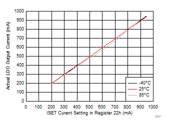
Actual Fast-charging Current vs Register Setting Across Device Temperature Range
4 Revision History
Changes from * Revision (September 2012) to A Revision
- Changed this data sheet to new SDS format plus replaced all text, tables and graphics. Go