SLLS413L February 2000 – June 2017 TUSB2046B , TUSB2046I
PRODUCTION DATA.
- 1 Features
- 2 Applications
- 3 Description
- 4 Revision History
- 5 Description (Continued)
- 6 Pin Configuration and Functions
- 7 Specifications
- 8 Detailed Description
- 9 Application and Implementation
- 10Power Supply Recommendations
- 11Layout
- 12Device and Documentation Support
- 13Mechanical, Packaging, and Orderable Information
Package Options
Mechanical Data (Package|Pins)
- VF|32
Thermal pad, mechanical data (Package|Pins)
Orderable Information
8 Detailed Description
8.1 Overview
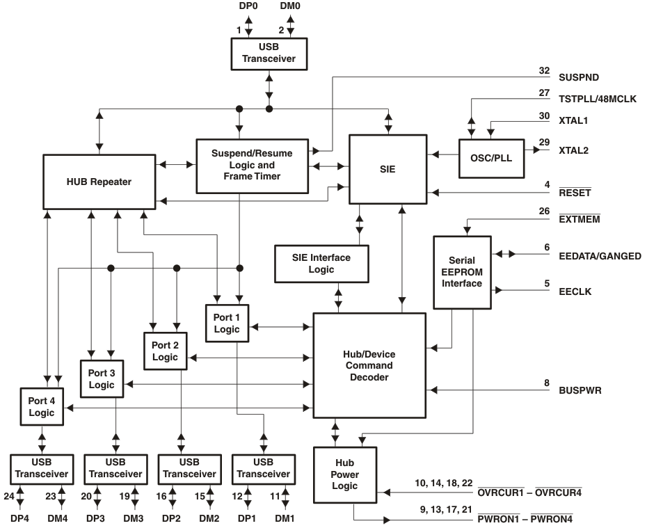
The TUSB2046x is a 3.3-V CMOS hub device that provides one upstream port and four downstream ports in compliance with the Universal Serial Bus (USB) specification as a full-speed hub. Because this device is implemented with a digital state machine instead of a microcontroller, no firmware programming is required. Fully compliant USB transceivers are integrated into the ASIC for all upstream and downstream ports. The downstream ports support full-speed and low-speed devices by automatically setting the slew rate according to the speed of the device attached to the ports. The configuration of the BUSPWR pin selects either the bus-powered or the self-powered mode.
8.2 Functional Block Diagram

8.3 Feature Description
8.3.1 USB Power Management
External power-management devices, such as the TPS2044, are required to control the 5-V source to the downstream ports according to the corresponding values of the PWRON pin. Upon detecting any overcurrent conditions, the power-management device sets the corresponding OVRCUR pin of the TUSB2046x to a logic low. If GANGED is high, all PWRON outputs switch together and if any OVRCUR is activated, all ports transition to the power-off state. If GANGED is low, the PWRON outputs and OVRCUR inputs operate on a per-port basis.
Both bus-powered and self-powered hubs require overcurrent protection for all downstream ports. The two types of protection are individual-port management (individual-port basis) or ganged-port management (multiple-port basis). Individual-port management requires power-management devices for each individual downstream port, but adds robustness to the USB system because, in the event of an overcurrent condition, the USB host only powers down the port that has the condition. The ganged configuration uses fewer power-management devices and thus has lower system costs, but in the event of an overcurrent condition on any of the downstream ports, all the ganged ports are disabled by the USB host.
Using a combination of the BUSPWR and EEDATA/GANGED inputs, the TUSB2046x supports four modes of power management: bus-powered hub with either individual-port power-management or ganged-port power management, and the self-powered hub with either individual-port power management or ganged-port power management. TI supplies the complete hub solution with the TUSB2036 (2/3-port), TUSB2046x, and the TUSB2077 (7-port) hubs along with the power-management devices needed to implement a fully USB specification-compliant system.
8.3.2 Clock Generation
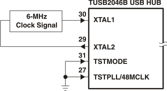
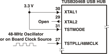
The input clock configuration logic of TUSB2046x is enhanced to accept a 6-MHz crystal or 48-MHz on-the-board clock source with a simple tie-off change on TSTMODE (pin 31).
- A 6-MHz input clock configuration is shown in Figure 5.
- A 48-MHz input clock configuration is shown in Figure 7.
In this mode, both TSTMODE and TSTPLL/48MCLK pins must be tied to ground. The hub is configured to use the 6-MHz clock on pins 30 and 29, which are XTAL1 and XTAL2, respectively, on the TUSB2046x. This is identical to the TUSB2046.
 Figure 5. 6-MHz Input Clock Configuration

NOTE:
This figure assumes a 6-MHz fundamental crystal that is parallel loaded. The component values of C1, C2, and Rd are determined using a crystal from Fox Electronics – part number HC49U-6.00MHz 30\50\0-70\20, which means ±30 ppm at 25°C and ±50 ppm from 0°C to 70°C. The characteristics for the crystal include a load capacitance (CL) of 20 pF, maximum shunt capacitance (Co) of 7 pF, and the maximum ESR of 50 Ω. In order to insure enough negative resistance, use C1 = C2 = 27 pF. The resistor Rd is used to trim the gain, and Rd = 1.5 kΩ is recommended.In this mode, both TSTMODE and XTAL1 pins must be tied to 3.3-V VCC. The hub accepts the 48-MHz clock input on TSTPLL/48MCLK (terminal 27). XTAL2 must be left floating (open) for this configuration. Only the oscillator or the onboard clock source is accepted for this mode. A crystal cannot be used for this mode, because the internal oscillator cell of the chip only supports the fundamental frequency.
 Figure 7. 48-MHz Input Clock Configuration
8.4 Device Functional Modes
8.4.1 Vendor ID and Product ID With External Serial EEPROM
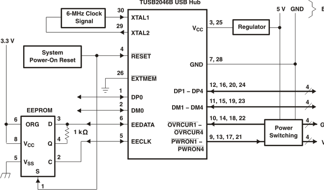
The EXTMEM pin enables or disables the optional EEPROM interface. When the EXTMEM pin is high, the product ID (PID) displayed during enumeration is the general-purpose USB hub. For this default, pin 5 is disabled and pin 6 functions as the GANGED input pin. If custom product ID (PID) and vendor ID (VID) descriptors are desired, the EXTMEM pin must be low (EXTMEM = 0). For this configuration, pins 5 and 6 function as the EEPROM interface with pins 5 and 6 functioning as EECLK and EEDATA, respectively. See Table 1 for a description of the EEPROM memory map. A block diagram example of how to connect the external EEPROM if a custom PID and VID are desired is shown in Figure 8.
 Figure 8. Typical Application of the TUSB2046x USB Hub
8.5 Programming
An SGS Thompson M93C46 EEPROM, or equivalent, stores the programmable VID and PID. When the EEPROM interface is enabled (EXTMEM = 0), the EECLK and EEDATA are internally pulled down (100 μA) inside the TUSB2046x. The internal pulldowns are disabled when the EEPROM interface is disabled (EXTMEM = 1).
The EEPROM is programmed with the three 16-bit locations as shown in Table 1. Connecting terminal 6 of the EEPROM high (ORG = 1) organizes the EEPROM memory into 64×16-bit words.
Table 1. EEPROM Memory Map
| ADDRESS | D15 | D14 | D13 | D12–D8 | D7–D0 |
|---|---|---|---|---|---|
| 00000 | 0 | GANGED | 00000 | 00000 | 00000000 |
| 00001 | VID high-byte | VID low-byte | |||
| 00010 | PID high-byte | PID low-byte | |||
| XXXXXXXX | |||||
The D and Q signals of the EEPROM must be tied together using a 1-kΩ resistor with the common I/O operations forming a single-wire bus. After system power-on reset, the TUSB2046x performs a one-time access read operation from the EEPROM if the EXTMEM terminal is pulled low and the chip select(s) of the EEPROM is connected to the system power-on reset. Initially, the EEDATA terminal is driven by the TUSB2046x to send a start bit (1) which is followed by the read instruction (10) and the starting-word address (00000). Once the read instruction is received, the instruction and address are decoded by the EEPROM, which then sends the data to the output shift register. At this point, the hub stops driving the EEDATA terminal and the EEPROM starts driving. A dummy (0) bit is then output and the first three 16-bit words in the EEPROM are output with the most significant bit (MSB) first.
The output data changes are triggered by the rising edge of the clock provided by the TUSB2046x on the EECLK terminal. The SGS-Thompson M936C46 EEPROM is recommended because it advances to the next memory location by automatically incrementing the address internally. Any EEPROM used must have the automatic internal address advance function. After reading the three words of data from the EEPROM, the TUSB2046x puts the EEPROM interface into a high-impedance condition (pulled down internally) to allow other logic to share the EEPROM. The EEPROM read operation is summarized in Figure 9. For more details on EEPROM operation, refer to SGS-Thompson Microelectronics M93C46 Serial Microwire Bus EEPROM data sheet.
 Figure 9. EEPROM Read Operation Timing Diagram