SLVSDO2C February   2017  – February 2018 TVS3300

PRODUCTION DATA.  

  1. Features
  2. Applications
  3. Description
    1.     Device Images
      1.      Footprint Comparison
      2.      Voltage Clamp Response to 8/20 µs Surge Event
  4. Revision History
  5. Device Comparison Table
  6. Pin Configuration and Functions
    1.     Pin Functions
  7. Specifications
    1. 7.1 Absolute Maximum Ratings
    2. 7.2 ESD Ratings - JEDEC
    3. 7.3 ESD Ratings - IEC
    4. 7.4 Recommended Operating Conditions
    5. 7.5 Thermal Information
    6. 7.6 Electrical Characteristics
    7. 7.7 Typical Characteristics
  8. Detailed Description
    1. 8.1 Overview
    2. 8.2 Functional Block Diagram
    3. 8.3 Feature Description
    4. 8.4 Reliability Testing
    5. 8.5 Device Functional Modes
      1. 8.5.1 Protection Specifications
      2. 8.5.2 Minimal Derating
      3. 8.5.3 Transient Performance
  9. Application and Implementation
    1. 9.1 Application Information
    2. 9.2 Typical Application
      1. 9.2.1 Design Requirements
      2. 9.2.2 Detailed Design Procedure
      3. 9.2.3 PLC Surge Protection Reference Design
      4. 9.2.4 Configuration Options
  10. 10Power Supply Recommendations
  11. 11Layout
    1. 11.1 Layout Guidelines
    2. 11.2 Layout Example
  12. 12Device and Documentation Support
    1. 12.1 Documentation Support
      1. 12.1.1 Related Documentation
    2. 12.2 Receiving Notification of Documentation Updates
    3. 12.3 Community Resources
    4. 12.4 Trademarks
    5. 12.5 Electrostatic Discharge Caution
    6. 12.6 Glossary
  13. 13Mechanical, Packaging, and Orderable Information

Package Options

Mechanical Data (Package|Pins)
Thermal pad, mechanical data (Package|Pins)
Orderable Information

Pin Configuration and Functions

YZF Package
4-Pin WCSP
Top View
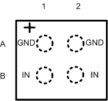
TVS3300 YZF_SLVSDO2.gif
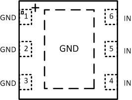
DRV Package
6-Pin SON
Top View
TVS3300 DRV_TVS3300.gif

Pin Functions

PINTYPEDESCRIPTION
NAME YZFDRV
IN B1, B2 4, 5, 6 I ESD and surge protected channel
GND A1, A2 1, 2, 3, exposed thermal pad GND Ground