SLUS873C January 2009 – December 2016 UC1825A-SP
PRODUCTION DATA.
- 1 Features
- 2 Applications
- 3 Description
- 4 Revision History
- 5 Description (continued)
- 6 Pin Configuration and Functions
- 7 Specifications
- 8 Detailed Description
-
9 Application and Implementation
- 9.1 Application Information
- 9.2
Typical Application
- 9.2.1 Design Requirements
- 9.2.2
Detailed Design Procedure
- 9.2.2.1 Auxiliary Supply Voltage
- 9.2.2.2 Oscillator Frequency
- 9.2.2.3 Preliminary Considerations
- 9.2.2.4 Input Power
- 9.2.2.5 Primary Current
- 9.2.2.6 Sense Resistor R(s)
- 9.2.2.7 MOSFET DC Losses
- 9.2.2.8 Selection of Core Material
- 9.2.2.9 Main Transformer Design
- 9.2.2.10 Calculation of Transformer
- 9.2.2.11 Minimum Core Size
- 9.2.2.12 Core Loss Limited Conditions
- 9.2.2.13 Core Geometry Selection
- 9.2.2.14 Wire Size Selection
- 9.2.2.15 Calculate Secondary RMS Current
- 9.2.2.16 Transformer Assembly
- 9.2.2.17 Calculation of Winding Resistances and Losses
- 9.2.2.18 Transformer Power Losses
- 9.2.2.19 Output Section
- 9.2.2.20 UC1825A-SP PWM Control Section
- 9.2.2.21 Closing the Feedback Loop
- 9.2.2.22 Summary
- 9.2.3 Application Curves
- 10Power Supply Recommendations
- 11Layout
- 12Device and Documentation Support
- 13Mechanical, Packaging, and Orderable Information
Package Options
Mechanical Data (Package|Pins)
Thermal pad, mechanical data (Package|Pins)
Orderable Information
1 Features
- QML-V Qualified, SMD 5962-87681
- 5962P8768105Vxx:
- Radiation Hardness Assurance (RHA) up to
30-krad(Si) Total Ionizing Dose (TID) - Passes Functional and Specified Post-Radiation Parametric Limits at 45 krad at LDR (10 mrad(Si)/s) per 1.5× Over Test as Defined in MIL-STD-883 Test Method 1019.9 Paragraph 3.13.3.b
- Exhibits Low Dose Rate Sensitivity but Remains Within the Pre-Radiation Electrical Limits at 30-krad Total Dose Level, as Allowed by MIL-STD-883, TM1019
- Radiation Hardness Assurance (RHA) up to
- Compatible With Voltage-Mode or Current-Mode Control Methods
- Practical Operation at Switching Frequencies
to 1 MHz - 50-ns Propagation Delay to Output
- High-Current Dual Totem Pole Outputs
(2-A Peak) - Trimmed Oscillator Discharge Current
- Low 100-μA Start-Up Current
- Pulse-by-Pulse Current Limiting Comparator
- Latched Overcurrent Comparator With Full Cycle Restart
- Qualified Over the Military Temperature Range (–55°C to 125°C)
2 Applications
- Radiation-Hardened DC-DC Converters
- Satellite Buses and Payloads
- Space Launch Vehicles
- Undersea Cabling
- Supports Various Topologies:
- Flyback, Forward, Buck, Boost
- Push-Pull, Half-Bridge, Full Bridge With External Interface Circuit
3 Description
The UC1825A-SP PWM controller is a radiation hardened version of the standard UC1825 family. Performance enhancements have been made to several of the circuit blocks. Error amplifier gain bandwidth product is 12 MHz, while input offset voltage is 2 mV. Current limit threshold is assured to a tolerance of 5%. Oscillator discharge current is specified at 10 mA for accurate dead time control. Frequency accuracy is improved to 6%. Start-up supply current, typically
100 μA, is ideal for offline applications. The output drivers are redesigned to actively sink current during UVLO at no expense to the start-up current specification. In addition each output is capable of
2-A peak currents during transitions.
Device Information(1)
| PART NUMBER | PACKAGE | BODY SIZE (NOM) |
|---|---|---|
| UC1825A-SP | CDIP (16) | 19.56 mm × 6.92 mm |
| UC1825A-SP RHA | CDIP (16) | 19.56 mm × 6.92 mm |
| CFP (16) | 10.16 mm × 7.10 mm |
- For all available packages, see the orderable addendum at the end of the data sheet.
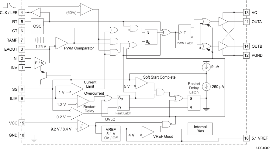
Block Diagram
