SLUSAF9B February 2011 – July 2015 UCC27200A , UCC27201A
PRODUCTION DATA.
- 1 Features
- 2 Applications
- 3 Description
- 4 Revision History
- 5 Pin Configuration and Functions
- 6 Specifications
- 7 Detailed Description
- 8 Application and Implementation
- 9 Power Supply Recommendations
- 10Layout
- 11Device and Documentation Support
- 12Mechanical, Packaging, and Orderable Information
Package Options
Mechanical Data (Package|Pins)
Thermal pad, mechanical data (Package|Pins)
Orderable Information
1 Features
- Drives Two N-Channel MOSFETs in High-Side and Low-Side Configuration
- Negative Voltage Handling on HS (–18V)
- Maximum Boot Voltage 120 V
- Maximum VDD Voltage 20 V
- On-Chip 0.65-V VF, 0.6-Ω RD Bootstrap Diode
- Greater than 1 MHz of Operation
- 20-ns Propagation Delay Times
- 3-A Sink, 3-A Source Output Currents
- 8-ns Rise/7-ns Fall Time with 1000-pF Load
- 1-ns Delay Matching
- Undervoltage Lockout for High-Side and Low-Side Driver
- Offered in 8-Pin SOIC (D), PowerPAD™ SOIC-8 (DDA), SON-8 (DRM), SON-9 (DRC) and SON-10 (DPR) Packages
- Specified from –40°C to 140°C
2 Applications
- Power Supplies for Telecom, Datacom, and Merchant Markets
- Half-Bridge Applications and Full-Bridge Converters
- Isolated Bus Architecture
- Two-Switch Forward Converters
- Active-Clamp Forward Converters
- High-Voltage Synchronous-Buck Converters
- Class-D Audio Amplifiers
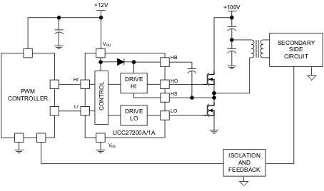
Simplified Application Diagram

3 Description
The UCC2720xA family of high-frequency N-channel MOSFET drivers include a 120-V bootstrap diode and high-side/low-side driver with independent inputs for maximum control flexibility. This allows for N-channel MOSFET control in half-bridge, full-bridge, two-switch forward and active clamp forward converters. The low-side and the high-side gate drivers are independently controlled and matched to 1-ns between the turn-on and turn-off of each other. The UCC2720xA are based on the popular UCC27200/1 drivers, but offer some enhancements. In order to improve performance in noisy power supply environments the UCC2720xA has an enhanced ESD input structure and also has the ability to withstand a maximum of –18 V on its HS pin.
An on-chip bootstrap diode eliminates the external discrete diodes. Under-voltage lockout is provided for both the high-side and the low-side drivers forcing the outputs low if the drive voltage is below the specified threshold.
Two versions of the UCC27200A are offered. The UCC27200A has high-noise immune CMOS input thresholds while the UCC27201A has TTL-compatible thresholds.
Both devices are offered in an 8-pin SOIC (D), PowerPad SOIC-8 (DDA), SON-8 (DRM) package, a 9-pin SON-9 (DRC) package and a 10-pin SON-10 (DPR) package.
Device Information(1)
| PART NUMBER | PACKAGE | BODY SIZE (NOM) |
|---|---|---|
| UCC27200A, UCC27201A |
SOIC (8) | 4.90 mm × 3.91 mm |
| HSOP (8) | 4.89 mm × 3.90 mm | |
| VSON (9) | 3.00 mm × 3.00 mm | |
| VSON (8) | 4.00 mm × 4.00 mm | |
| UCC27201A | WSON (10) | 4.00 mm × 4.00 mm |
- For all available packages, see the orderable addendum at the end of the data sheet.