SLUSCZ8 July 2017 UCC27212A-Q1
PRODUCTION DATA.
- 1 Features
- 2 Applications
- 3 Description
- 4 Revision History
- 5 Pin Configuration and Functions
- 6 Specifications
- 7 Detailed Description
- 8 Application and Implementation
- 9 Power Supply Recommendations
- 10Layout
- 11Device and Documentation Support
- 12Mechanical, Packaging, and Orderable Information
Package Options
Mechanical Data (Package|Pins)
- DDA|8
Thermal pad, mechanical data (Package|Pins)
- DDA|8
Orderable Information
1 Features
- Qualified for Automotive Applications
- AECA-Q100 Qualified with the following results:
- Device temperature grade –40°C to +140°C
- Device HBM classification level 2
- Device CDM classification level C6
- 5-V Turn-off Under Voltage Lockout (UVLO)
- Drives Two N-Channel MOSFETs in High-Side and Low-Side Configuration With Independent Inputs
- Maximum Boot Voltage 120-V DC
- 4-A Sink, 4-A Source Output Currents
- 0.9-Ω Pullup and Pulldown Resistance
- Input Pins Can Tolerate –10 V to +20 V and are Independent of Supply Voltage Range
- TTL Compatible Inputs
- 5-V to 17-V VDD Operating Range, (20-V ABS Maximum)
- 7.2-ns Rise and 5.5-ns Fall Time With 1000-pF Load
- Fast Propagation Delay Times (20-ns typical)
- 4-ns Typical Delay Matching
- Available in the SOIC8(Powerpad) package
2 Applications
- Power Supplies in Automotive Applications
- Half-Bridge and Full-Bridge Converters
- High-Voltage Synchronous-Buck Converters
- Two-Switch Forward Converters
- Push-Pull and Active-Clamp Forward Converters
- Class-D Audio Amplifiers
3 Description
The UCC27212A-Q1 device driver is based on the popular UCC27211 MOSFET drivers. In addition, UCC27212A-Q1 offers extended operating range all the way down to 5 V which helps lower power losses.
The peak output pullup and pulldown current is 4-A source and 4-A sink, and pullup and pulldown resistance is 0.9 Ω. This allows for the ability to drive large power MOSFETs with minimized switching losses during the transition through the Miller Plateau of the MOSFET.
The input structure can directly handle –10 V, which increases robustness and also allows direct interface to gate-drive transformers without using rectification diodes. The inputs are also independent of supply voltage and have a 20-V maximum rating.
The switching node of the UCC27212A-Q1 (HS pin) can handle –18-V maximum, which allows the high-side channel to be protected from inherent negative voltages caused by parasitic inductance and stray capacitance. The UCC27212A-Q1 has increased hysteresis that allows for interface to analog or digital PWM controllers with enhanced noise immunity.
The low-side and high-side gate drivers are independently controlled and matched to 4 ns between the turn on and turn off of each other.
An on-chip 100-V rated bootstrap diode eliminates the external discrete diodes. Undervoltage lockout is provided for both the high-side and the low-side drivers which provides symmetric turn on and turn off behavior and forces the outputs low if the drive voltage is below the specified threshold.
Device Information(1)
| PART NUMBER | PACKAGE | BODY SIZE (NOM) |
|---|---|---|
| UCC27212A-Q1 | SOIC8(Powerpad) | 5.0 mm x 6.0 mm |
- For all available packages, see the orderable addendum at the end of the data sheet.
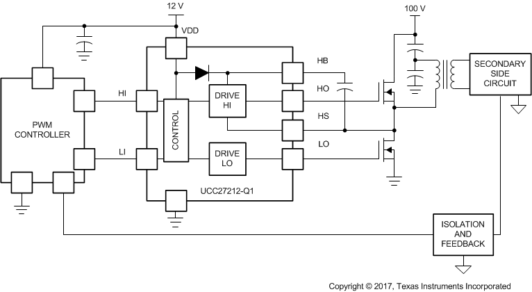
Typical Application Diagram

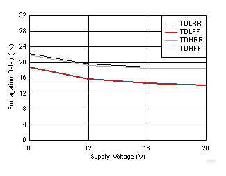
Propagation Delays vs Supply Voltage T = 25°C
