SLUSCZ8 July 2017 UCC27212A-Q1
PRODUCTION DATA.
- 1 Features
- 2 Applications
- 3 Description
- 4 Revision History
- 5 Pin Configuration and Functions
- 6 Specifications
- 7 Detailed Description
- 8 Application and Implementation
- 9 Power Supply Recommendations
- 10Layout
- 11Device and Documentation Support
- 12Mechanical, Packaging, and Orderable Information
Package Options
Mechanical Data (Package|Pins)
- DDA|8
Thermal pad, mechanical data (Package|Pins)
- DDA|8
Orderable Information
8 Application and Implementation
NOTE
Information in the following applications sections is not part of the TI component specification, and TI does not warrant its accuracy or completeness. TI’s customers are responsible for determining suitability of components for their purposes. Customers should validate and test their design implementation to confirm system functionality.
8.1 Application Information
To affect fast switching of power devices and reduce associated switching power losses, a powerful gate driver is employed between the PWM output of controllers and the gates of the power semiconductor devices. Also, gate drivers are indispensable when it is impossible for the PWM controller to directly drive the gates of the switching devices. With the advent of digital power, this situation will be often encountered because the PWM signal from the digital controller is often a 3.3-V logic signal which cannot effectively turn on a power switch. Level shifting circuitry is needed to boost the 3.3-V signal to the gate-drive voltage (such as 12 V) in order to fully turn on the power device and minimize conduction losses. Traditional buffer drive circuits based on NPN/PNP bipolar transistors in totem-pole arrangement, being emitter follower configurations, prove inadequate with digital power because they lack level-shifting capability. Gate drivers effectively combine both the level-shifting and buffer-drive functions. Gate drivers also find other needs such as minimizing the effect of high-frequency switching noise by locating the high-current driver physically close to the power switch, driving gate-drive transformers, and controlling floating power-device gates, reducing power dissipation and thermal stress in controllers by moving gate charge power losses from the controller into the driver.
Finally, emerging wide band-gap power device technologies such as GaN based switches, which are capable of supporting very high switching frequency operation, are driving very special requirements in terms of gate drive capability. These requirements include operation at low VDD voltages (5 V or lower), low propagation delays and availability in compact, low-inductance packages with good thermal capability. Gate-driver devices are extremely important components in switching power, and they combine the benefits of high-performance, low-cost component count and board-space reduction as well as simplified system design.
8.2 Typical Application
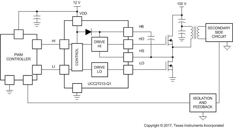
 Figure 19. UCC27212A-Q1 Typical Application
8.2.1 Design Requirements
For this design example, use the parameters listed in Table 3.
Table 3. Design Specifications
| DESIGN PARAMETER | EXAMPLE VALUE |
|---|---|
| Supply voltage, VDD | 12 V |
| Voltage on HS, VHS | 0 V to 100 V |
| Voltage on HB, VHB | 12 V to 112 V |
| Output current rating, IO | –4 A to 4 A |
| Operating frequency | 500 kHz |
8.2.2 Detailed Design Procedure
8.2.2.1 Power Dissipation
Power dissipation of the gate driver has two portions as shown in Equation 1.
Use Equation 2 to calculate the DC portion of the power dissipation (PDC).
where
- IQ is the quiescent current for the driver.
The quiescent current is the current consumed by the device to bias all internal circuits such as input stage, reference voltage, logic circuits, protections, and also any current associated with switching of internal devices when the driver output changes state (such as charging and discharging of parasitic capacitances, parasitic shoot-through, and so forth). The UCC27212A-Q1 features very low quiescent currents (less than 0.17 mA, refer to the table and contain internal logic to eliminate any shoot-through in the output driver stage. Thus the effect of the PDC on the total power dissipation within the gate driver can be safely assumed to be negligible. The power dissipated in the gate-driver package during switching (PSW) depends on the following factors:
- Gate charge required of the power device (usually a function of the drive voltage VG, which is very close to input bias supply voltage VDD)
- Switching frequency
- Use of external gate resistors. When a driver device is tested with a discrete, capacitive load calculating the power that is required from the bias supply is fairly simple. The energy that must be transferred from the bias supply to charge the capacitor is given by Equation 3.
- CLOAD is load capacitor
- VDD is bias voltage feeding the driver
where
There is an equal amount of energy dissipated when the capacitor is charged and when it is discharged. This leads to a total power loss given by Equation 4.
where
- fSW is the switching frequency
The switching load presented by a power MOSFET/IGBT is converted to an equivalent capacitance by examining the gate charge required to switch the device. This gate charge includes the effects of the input capacitance plus the added charge needed to swing the drain voltage of the power device as it switches between the ON and OFF states. Most manufacturers provide specifications of typical and maximum gate charge, in nC, to switch the device under specified conditions. Using the gate charge Qg, determine the power that must be dissipated when switching a capacitor which is calculated using the equation QG = CLOAD × VDD to provide Equation 5 for power.
This power PG is dissipated in the resistive elements of the circuit when the MOSFET/IGBT is being turned on and off. Half of the total power is dissipated when the load capacitor is charged during turnon, and the other half is dissipated when the load capacitor is discharged during turnoff. When no external gate resistor is employed between the driver and MOSFET/IGBT, this power is completely dissipated inside the driver package. With the use of external gate-drive resistors, the power dissipation is shared between the internal resistance of driver and external gate resistor.
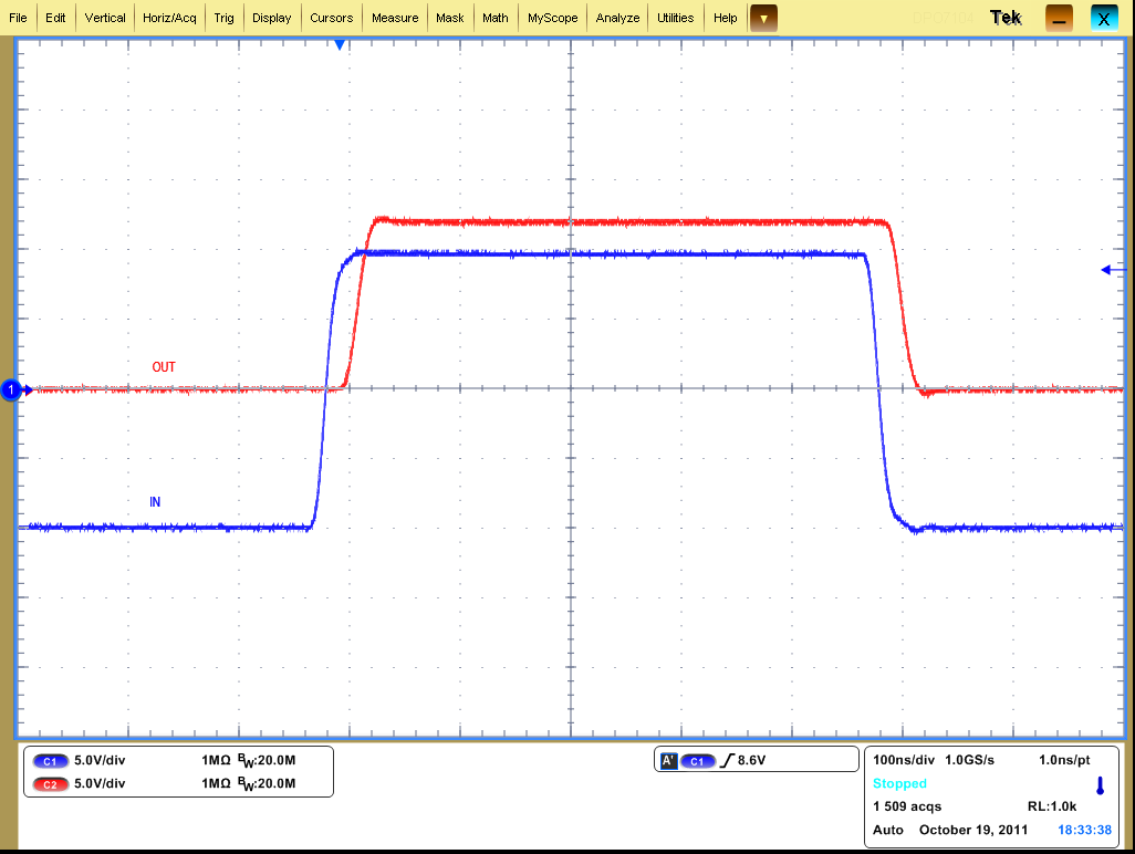
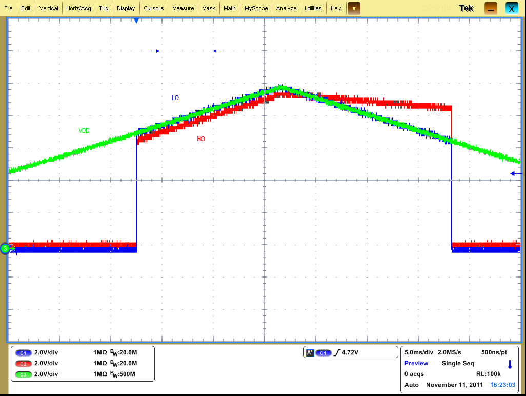
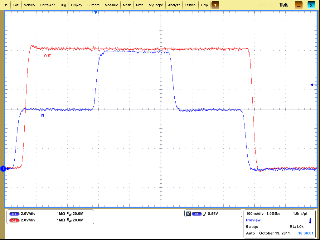
8.2.3 Application Curves


