SLUSCZ8 July 2017 UCC27212A-Q1
PRODUCTION DATA.
- 1 Features
- 2 Applications
- 3 Description
- 4 Revision History
- 5 Pin Configuration and Functions
- 6 Specifications
- 7 Detailed Description
- 8 Application and Implementation
- 9 Power Supply Recommendations
- 10Layout
- 11Device and Documentation Support
- 12Mechanical, Packaging, and Orderable Information
Package Options
Mechanical Data (Package|Pins)
- DDA|8
Thermal pad, mechanical data (Package|Pins)
- DDA|8
Orderable Information
6 Specifications
6.1 Absolute Maximum Ratings
over operating free-air temperature range (unless otherwise noted)(1)| MIN | MAX | UNIT | |||
|---|---|---|---|---|---|
| VDD(2), VHB – VHS | Supply voltage range | –0.3 | 20 | V | |
| VLI, VHI | Input voltages on LI and HI | –10 | 20 | V | |
| VLO | Output voltage on LO | DC | –0.3 | VDD + 0.3 | V |
| Repetitive pulse < 100 ns(3) | –2 | VDD + 0.3 | V | ||
| VHO | Output voltage on HO | DC | VHS – 0.3 | VHB + 0.3 | V |
| Repetitive pulse < 100 ns(3) | VHS – 2 | VHB + 0.3 | V | ||
| VHS | Voltage on HS | DC | –1 | 100 | V |
| Repetitive pulse < 100 ns(3) | –(24 V – VDD) | 115 | V | ||
| VHB | Voltage on HB | –0.3 | 120 | V | |
| TJ | Operating virtual junction temperature range | –40 | 150 | °C | |
| Storage temperature, Tstg | –65 | 150 | °C | ||
(1) Stresses beyond those listed under Absolute Maximum Ratings may cause permanent damage to the device. These are stress ratings only, which do not imply functional operation of the device at these or any other conditions beyond those indicated under Recommended Operating Conditions. Exposure to absolute-maximum-rated conditions for extended periods may affect device reliability.
(2) All voltages are with respect to VSS unless otherwise noted. Currents are positive into and negative out of the specified terminal.
(3) Verified at bench characterization. VDD is the value used in an application design.
6.2 ESD Ratings
| VALUE | UNIT | |||
|---|---|---|---|---|
| V(ESD) | Electrostatic discharge | Human-body model (HBM), per AEC Q100-002 | ±2000 | V |
| Charged-device model (CDM), per AEC Q100-011 | ±1500 | |||
6.3 Recommended Operating Conditions
over operating free-air temperature range, all voltages are with respect to VSS; currents are positive into and negative out of the specified terminal. –40°C < TJ = TA < 140°C (unless otherwise noted)| MIN | NOM | MAX | UNIT | ||
|---|---|---|---|---|---|
| VDD | Supply voltage range, VHB – VHS | 7 | 12 | 17 | V |
| VHS | Voltage on HS | –1 | 100 | V | |
| VHS | Voltage on HS (repetitive pulse < 100 ns) | –(20 V – VDD) | 110 | V | |
| VHB | Voltage on HB | VHS + 8 | 115 | V | |
| Voltage slew rate on HS | 50 | V/ns | |||
| Operating junction temperature | –40 | 140 | °C | ||
6.4 Thermal Information
| THERMAL METRIC(1) | UCC27212A-Q1 | UNIT | |
|---|---|---|---|
| DDA (SOIC8 Powerpad) | |||
| 8 PINS | |||
| RθJA | Junction-to-ambient thermal resistance | 37.7 | °C/W |
| RθJC(top) | Junction-to-case (top) thermal resistance | 47.2 | °C/W |
| RθJB | Junction-to-board thermal resistance | 9.6 | °C/W |
| ψJT | Junction-to-top characterization parameter | 2.8 | °C/W |
| ψJB | Junction-to-board characterization parameter | 9.4 | °C/W |
| RθJC(bot) | Junction-to-case (bottom) thermal resistance | 3.6 | °C/W |
(1) For more information about traditional and new thermal metrics, see the Semiconductor and IC Package Thermal Metrics application report.
6.5 Electrical Characteristics
over operating free-air temperature range, VHS = VSS = 0 V, no load on LO or HO, TA = TJ = –40°C to +140°C, (unless otherwise noted)| PARAMETER | TEST CONDITIONS | MIN | TYP | MAX | UNIT | |
|---|---|---|---|---|---|---|
| SUPPLY CURRENTS, VDD = VHB = 12 V | ||||||
| IDD | VDD quiescent current | V(LI) = V(HI) = 0 V | 0.05 | 0.085 | 0.17 | mA |
| IDDO | VDD operating current | f = 500 kHz, CLOAD = 0 | 2.1 | 2.5 | 6.5 | mA |
| IHB | Boot voltage quiescent current | V(LI) = V(HI) = 0 V | 0.015 | 0.065 | 0.1 | mA |
| IHBO | Boot voltage operating current | f = 500 kHz, CLOAD = 0 | 1.5 | 2.5 | 5.1 | mA |
| IHBS | HB to VSS quiescent current | V(HS) = V(HB) = 115 V | 0.0005 | 1 | µA | |
| IHBSO | HB to VSS operating current | f = 500 kHz, CLOAD = 0 | 0.07 | 1.2 | mA | |
| SUPPLY CURRENTS, VDD = VHB = 6.8 V | ||||||
| IDD | VDD quiescent current | V(LI) = V(HI) = 0 V | 0.02 | 0.065 | 0.14 | mA |
| IDDO | VDD operating current | f = 500 kHz, CLOAD = 0 | 0.7 | 1.4 | 6.5 | mA |
| IHB | Boot voltage quiescent current | V(LI) = V(HI) = 0 V | 0.01 | 0.04 | 0.08 | mA |
| IHBO | Boot voltage operating current | f = 500 kHz, CLOAD = 0 | 0.5 | 1.23 | 5.1 | mA |
| IHBS | HB to VSS quiescent current | V(HS) = V(HB) = 115 V | 0.0005 | 1 | µA | |
| IHBSO | HB to VSS operating current | f = 500 kHz, CLOAD = 0 | 0.07 | 1.2 | mA | |
| INPUT, VDD = VHB = 12 V | ||||||
| VHIT | Input voltage threshold | 1.7 | 2.3 | 2.55 | V | |
| VLIT | Input voltage threshold | 1.2 | 1.6 | 1.9 | V | |
| VIHYS | Input voltage hysteresis | 700 | mV | |||
| RIN | Input pulldown resistance | 68 | kΩ | |||
| INPUT, VDD = VHB = 6.8 V | ||||||
| VHIT | Input voltage threshold | 1.6 | 2.0 | 2.6 | V | |
| VLIT | Input voltage threshold | 1.1 | 1.5 | 2.1 | V | |
| VIHYS | Input voltage hysteresis | 500 | mV | |||
| RIN | Input pulldown resistance | 68 | kΩ | |||
| UNDER-VOLTAGE LOCKOUT (UVLO), VDD = VHB = 12 V | ||||||
| VDDR | VDD turnon threshold | 4.9 | 5.7 | 6.4 | V | |
| VDDHYS | Hysteresis | 0.4 | V | |||
| VHBR | VHB turnon threshold | 4.35 | 5.3 | 6.3 | V | |
| VHBHYS | Hysteresis | 0.3 | V | |||
| BOOTSTRAP DIODE, VDD = VHB = 12 V | ||||||
| VF | Low-current forward voltage | IVDD-HB = 100 µA | 0.65 | 0.8 | V | |
| VFI | High-current forward voltage | IVDD-HB = 100 mA | 0.85 | 0.95 | V | |
| RD | Dynamic resistance, ΔVF/ΔI | IVDD-HB = 100 mA and 80 mA | 0.3 | 0.5 | 0.85 | Ω |
| BOOTSTRAP DIODE, VDD = VHB = 6.8 V | ||||||
| VF | Low-current forward voltage | IVDD-HB = 100 µA | 0.65 | 0.8 | V | |
| VFI | High-current forward voltage | IVDD-HB = 100 mA | 0.85 | 0.95 | V | |
| RD | Dynamic resistance, ΔVF/ΔI | IVDD-HB = 100 mA and 80 mA | 0.3 | 0.5 | 0.85 | Ω |
| LO GATE DRIVER, VDD = VHB = 12 V | ||||||
| VLOL | Low-level output voltage | 0.05 | 0.1 | 0.19 | V | |
| VLOH | High level output voltage | 0.1 | 0.16 | 0.29 | V | |
| Peak pullup current(1) | 3.7 | A | ||||
| Peak pulldown current (1) | 4.5 | A | ||||
| LO GATE DRIVER, VDD = VHB = 6.8 V | ||||||
| VLOL | Low-level output voltage | ILO = 100 mA | 0.04 | 0.13 | 0.35 | V |
| VLOH | High level output voltage | ILO = –100 mA, VLOH = VDD – VLO | 0.12 | 0.23 | 0.42 | V |
| Peak pullup current | VLO = 0 V | 1.3 | A | |||
| Peak pulldown current | VLO = 12 V for VDD = 6.8V | 1.7 | A | |||
| HO GATE DRIVER, VDD = VHB = 12 V | ||||||
| VHOL | Low-level output voltage | 0.05 | 0.1 | 0.19 | V | |
| VHOH | High-level output voltage | 0.1 | 0.16 | 0.29 | V | |
| Peak pullup current (1) | 3.7 | A | ||||
| Peak pulldown current (1) | 4.5 | A | ||||
| HO GATE DRIVER, VDD = VHB = 6.8 V | ||||||
| VLOL | Low-level output voltage | IHO = 100 mA | 0.04 | 0.13 | 0.35 | V |
| VLOH | High level output voltage | IHO = –100 mA, VHOH = VHB – VHO | 0.12 | 0.23 | 0.42 | V |
| Peak pullup current | VHO = 0 V | 1.3 | A | |||
| Peak pulldown current | VHO = 12 V for VDD = 6.8V | 1.7 | A | |||
(1) Ensured by design.
6.6 Switching Characteristics
over operating free-air temperature range (unless otherwise noted)| PARAMETER | TEST CONDITIONS | MIN | TYP | MAX | UNIT | |
|---|---|---|---|---|---|---|
| PROPAGATION DELAYS, VDD = VHB = 12 V | ||||||
| TDLFF | VLI falling to VLO falling | CLOAD = 0 | 10 | 16 | 30 | ns |
| TDHFF | VHI falling to VHO falling | CLOAD = 0 | 10 | 16 | 30 | ns |
| TDLRR | VLI rising to VLO rising | CLOAD = 0 | 10 | 20 | 42 | ns |
| TDHRR | VHI rising to VHO rising | CLOAD = 0 | 10 | 20 | 42 | ns |
| PROPAGATION DELAYS, VDD = VHB = 6.8 V | ||||||
| TDLFF | VLI falling to VLO falling | CLOAD = 0 | 10 | 24 | 50 | ns |
| TDHFF | VHI falling to VHO falling | CLOAD = 0 | 10 | 24 | 50 | ns |
| TDLRR | VLI rising to VLO rising | CLOAD = 0 | 13 | 28 | 57 | ns |
| TDHRR | VHI rising to VHO rising | CLOAD = 0 | 13 | 28 | 57 | ns |
| DELAY MATCHING, VDD = VHB = 12 V | ||||||
| TMON | From HO OFF to LO ON | TJ = 25°C | 4 | 9.5 | ns | |
| TJ = –40°C to +140°C | 4 | 17 | ns | |||
| TMOFF | From LO OFF to HO ON | TJ = 25°C | 4 | 9.5 | ns | |
| TJ = –40°C to +140°C | 4 | 17 | ns | |||
| DELAY MATCHING, VDD = VHB = 6.8 V | ||||||
| TMON | From HO OFF to LO ON | TJ = 25°C | 8 | ns | ||
| TJ = –40°C to +140°C | 8 | 18 | ns | |||
| TMOFF | From LO OFF to HO ON | TJ = 25°C | 6 | ns | ||
| TJ = –40°C to +140°C | 6 | 18 | ns | |||
| OUTPUT RISE AND FALL TIME, VDD = VHB = 12 V | ||||||
| tR | LO rise time | CLOAD = 1000 pF, from 10% to 90% | 7.8 | ns | ||
| tR | HO rise time | CLOAD = 1000 pF, from 10% to 90% | 7.8 | ns | ||
| tF | LO fall time | CLOAD = 1000 pF, from 90% to 10% | 6.0 | ns | ||
| tF | HO fall time | CLOAD = 1000 pF, from 90% to 10% | 6.0 | ns | ||
| tR | LO, HO | CLOAD = 0.1 µF, (3 V to 9 V) | 0.36 | 0.6 | µs | |
| tF | LO, HO | CLOAD = 0.1 µF, (9 V to 3 V) | 0.20 | 0.4 | µs | |
| OUTPUT RISE AND FALL TIME, VDD = VHB = 6.8 V | ||||||
| tR | LO rise time | CLOAD = 1000 pF, from 10% to 90% | 9.5 | ns | ||
| tR | HO rise time | CLOAD = 1000 pF, from 10% to 90% | 13.0 | ns | ||
| tF | LO fall time | CLOAD = 1000 pF, from 90% to 10% | 9.5 | ns | ||
| tF | HO fall time | CLOAD = 1000 pF, from 90% to 10% | 13.0 | ns | ||
| tR | LO, HO | CLOAD = 0.1 µF, (30% to 70%) | 0.45 | 0.7 | µs | |
| tF | LO, HO | CLOAD = 0.1 µF, (70% to 30%) | 0.2 | 0.5 | µs | |
| MISCELLANEOUS | ||||||
| Minimum input pulse width that changes the output | 100 | ns | ||||
| Bootstrap diode turnoff time (1)(2) | IF = 20 mA, IREV = 0.5 A (3) | 20 | ns | |||
| Extended output pulse | when VDD = VHB = 6.8 V, VHS = 100 V, and input pulse width is 100 ns | 250 | ns | |||
(1) Ensured by design.
(2) IF: Forward current applied to bootstrap diode, IREV: Reverse current applied to bootstrap diode.
(3) Typical values for TA = 25°C.
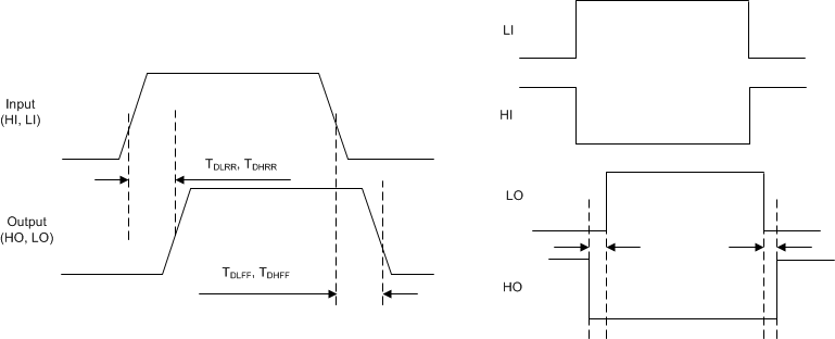 Figure 1. Timing Diagram
6.7 Typical Characteristics
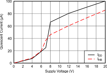
| T = 25°C |
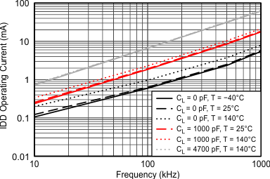
| VDD = 12 V |
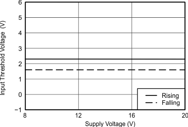
| T = 25°C |
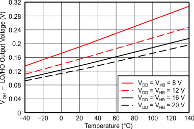
| IHO = ILO = 100 mA |
vs Temperature
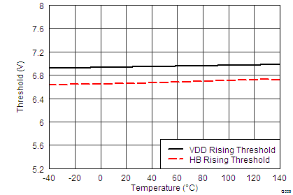
vs Temperature
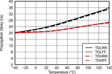
| VDD = VHB = 12 V |
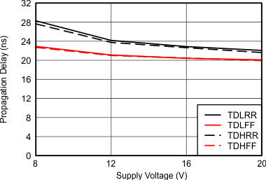
| T = 25°C |
(VDD = VHB)
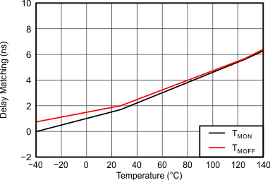
| VDD = VHB = 12 V |
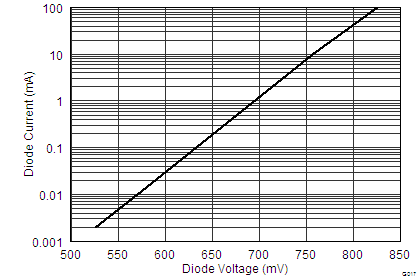
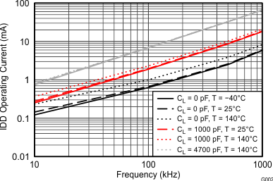
| VDD = 12 V |
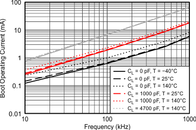
| VHB – VHS = 12 V |
Frequency (HB To HS)
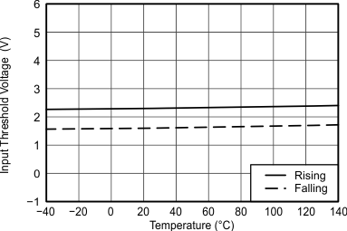
| VDD = 12 V |
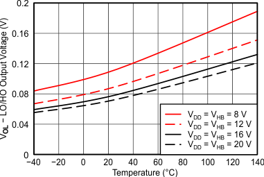
| IHO = ILO = 100 mA |
vs Temperature
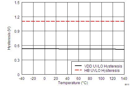
vs Temperature
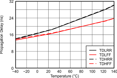
| VDD = VHB = 12 V |
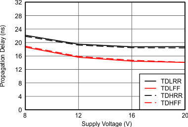
| T = 25°C |
(VDD = VHB)
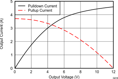
| VDD = VHB = 12 V |