SLUSCW3 August 2017 UCC27712-Q1
PRODUCTION DATA.
- 1 Features
- 2 Applications
- 3 Description
- 4 Simplified Schematic
- 5 Revision History
- 6 Pin Configuration and Functions
- 7 Specifications
- 8 Detailed Description
-
9 Application and Implementation
- 9.1 Application Information
- 9.2
Typical Application
- 9.2.1 Design Requirements
- 9.2.2
Detailed Design Procedure
- 9.2.2.1 Selecting HI and LI Low Pass Filter Components (RHI, RLI, CHI, CLI)
- 9.2.2.2 Selecting Bootstrap Capacitor (CBOOT)
- 9.2.2.3 Selecting VDD Bypass/Holdup Capacitor (CVDD) and Rbias
- 9.2.2.4 Selecting Bootstrap Resistor (RBOOT)
- 9.2.2.5 Selecting Gate Resistor RON/ROFF
- 9.2.2.6 Selecting Bootstrap Diode
- 9.2.2.7 Estimate the UCC27712-Q1 Power Losses (PUCC27712-Q1)
- 9.2.2.8 Estimating Junction Temperature
- 9.2.2.9 Operation With IGBT's
- 9.2.3 Application Curves
- 10Power Supply Recommendations
- 11Layout
- 12Device and Documentation Support
- 13Mechanical, Packaging, and Orderable Information
Package Options
Mechanical Data (Package|Pins)
- D|8
Thermal pad, mechanical data (Package|Pins)
Orderable Information
1 Features
- AEC-Q100 Qualified for Automotive Application
- Device HBM Classification Level 1C
- Device CDM Classification Level C4B
- High-Side and Low-Side Configuration
- Dual Inputs With Output Interlock and 150-ns Deadtime
- Fully Operational up to 620-V, 700-V Absolute Maximum on HB Pin
- 10-V to 20-V VDD Recommended Range
- Peak Output Current 2.8-A Sink, 1.8-A Source
- dv/dt Immunity of 50 V/ns
- Logic Operational up to –11 V on HS Pin
- Negative Voltage Tolerance On Inputs of –5 V
- Large Negative Transient Safe Operating Area
- UVLO Protection for Both Channels
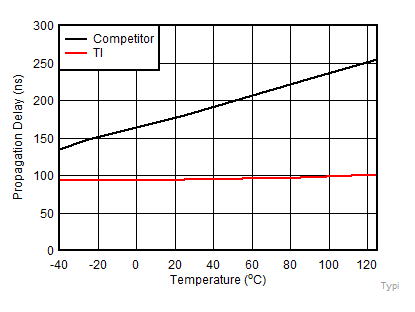
- Small Propagation Delay (100-ns Typical)
- Delay Matching (12-ns Typical)
- Low Quiescent Current
- TTL and CMOS Compatible Inputs
- Industry Standard SOIC-8 Package
- All Parameters Specified Over Temperature Range, –40 °C to +125 °C
2 Applications
- Automotive Inverters
- On-Board Chargers (PFC, Phase-Shifted Full Bridge)
- Motor Drive for Automotive Applications (Stepper Motors, Fans)
3 Description
The UCC27712-Q1 is a 620-V high-side and low-side gate driver with 1.8-A source, 2.8-A sink current, targeted to drive power MOSFETs or IGBTs.
The recommended VDD operating voltage is 10-V to 20-V for IGBT's and 10-V to 17-V for power MOSFETs.
The UCC27712-Q1 includes protection features where the outputs are held low when the inputs are left open or when the minimum input pulse width specification is not met. Interlock and deadtime functions prevent both outputs from being turned on simultaneously. In addition, the device accepts a wide range bias supply range from 10 V to 22 V, and offers UVLO protection for both the VDD and HB bias supply.
Developed with TI's state of the art high-voltage device technology, the device features robust drive with excellent noise and transient immunity including large negative voltage tolerance on its inputs, high dV/dt tolerance, wide negative transient safe operating area (NTSOA) on the switch node (HS), and interlock.
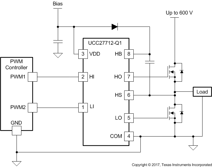
The device consists of one ground-referenced channel (LO) and one floating channel (HO) which is designed for operating with bootstrap or isolated power supplies. The device features fast propagation delays and excellent delay matching between both channels. On the UCC27712-Q1, each channel is controlled by its respective input pins, HI and LI.
Device Information(1)
| PART NUMBER | PACKAGE | BODY SIZE (NOM) |
|---|---|---|
| UCC27712-Q1 | SOIC (8) | 3.91 mm × 8.65 mm |
4 Simplified Schematic

Typical Propagation Delay Comparison
