SLUSCW3 August 2017 UCC27712-Q1
PRODUCTION DATA.
- 1 Features
- 2 Applications
- 3 Description
- 4 Simplified Schematic
- 5 Revision History
- 6 Pin Configuration and Functions
- 7 Specifications
- 8 Detailed Description
-
9 Application and Implementation
- 9.1 Application Information
- 9.2
Typical Application
- 9.2.1 Design Requirements
- 9.2.2
Detailed Design Procedure
- 9.2.2.1 Selecting HI and LI Low Pass Filter Components (RHI, RLI, CHI, CLI)
- 9.2.2.2 Selecting Bootstrap Capacitor (CBOOT)
- 9.2.2.3 Selecting VDD Bypass/Holdup Capacitor (CVDD) and Rbias
- 9.2.2.4 Selecting Bootstrap Resistor (RBOOT)
- 9.2.2.5 Selecting Gate Resistor RON/ROFF
- 9.2.2.6 Selecting Bootstrap Diode
- 9.2.2.7 Estimate the UCC27712-Q1 Power Losses (PUCC27712-Q1)
- 9.2.2.8 Estimating Junction Temperature
- 9.2.2.9 Operation With IGBT's
- 9.2.3 Application Curves
- 10Power Supply Recommendations
- 11Layout
- 12Device and Documentation Support
- 13Mechanical, Packaging, and Orderable Information
Package Options
Mechanical Data (Package|Pins)
- D|8
Thermal pad, mechanical data (Package|Pins)
Orderable Information
9 Application and Implementation
NOTE
Information in the following Applications section is not part of the TI component specification, and TI does not warrant its accuracy or completeness. TI’s customers are responsible for determining suitability of components for their purposes. Customers should validate and test their design implementation to confirm system functionality.
9.1 Application Information
To effect fast switching of power devices and reduce associated switching power losses, a powerful gate driver is employed between the PWM output of controllers and the gates of the power semiconductor devices. Also, gate drivers are indispensable when it is impossible for the PWM controller to directly drive the gates of the switching devices. With the advent of digital power, this situation will be often encountered because the PWM signal from the digital controller is often a 3.3-V logic signal which cannot effectively turn on a power switch. Level shifting circuitry is needed to boost the 3.3-V signal to the gate-drive voltage (such as 12 V) in order to fully turn on the power device and minimize conduction losses. Traditional buffer drive circuits based on NPN/PNP bipolar transistors in totem-pole arrangement, being emitter follower configurations, prove inadequate with digital power because they lack level-shifting capability.
Gate drivers effectively combine both the level-shifting and buffer-drive functions. Gate drivers also find other needs such as minimizing the effect of high-frequency switching noise by locating the high-current driver physically close to the power switch, driving gate-drive transformers and controlling floating power-device gates, reducing power dissipation and thermal stress in controllers by moving gate charge power losses from the controller into the driver.
9.2 Typical Application
The circuit in Figure 44 shows a reference design example with UCC27712-Q1 driving a typical half-bridge configuration which could be used in several common power converter topologies such as synchronous buck, synchronous boost, half-bridge/full bridge isolated topologies, and motor drive applications.
For more information, please refer to Figure 44.
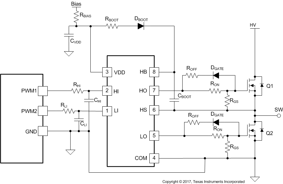 Figure 44. Typical Application Schematic
9.2.1 Design Requirements
Table 4 shows the reference design parameters for the example application: UCC27712-Q1 driving 650-V MOSFETs in a high side-low side configuration.
Table 4. UCC27712-Q1 Design Requirements
| PARAMETER | VALUE | UNIT | |
|---|---|---|---|
| Power transistor | IPB65R190CFD | - | |
| VDD | 12 | V | |
| Input signal amplitude | 3.3 | V | |
| Switching frequency (fSW) | 100 | kHz | |
| DC link voltage (VHV) | 400 | V | |
9.2.2 Detailed Design Procedure
This procedure outlines the steps to design a 600-V high-side, low-side gate driver with 1.8-A source and 2.8-A sink current capability, targeted to drive power MOSFETs or IGBTs using the UCC27712-Q1. Refer to Figure 44 for component names and network locations. For additional design help see the UCC27712EVM-287 User Guide, SLUUBO1.
9.2.2.1 Selecting HI and LI Low Pass Filter Components (RHI, RLI, CHI, CLI)
It is recommended that users avoid shaping the input signals to the gate driver in an attempt to slow down (or delay) the signal at the driver output. However it is good practice to have a small RC filter added between PWM controller and input pin of UCC27712-Q1 to filter the high frequency noise, like RHI/CHI and RLI/CLI which is shown in Figure 44.
Such a filter should use a RHI/RLI in the range of 10 Ω to 100 Ω and a CHI/CLI between 10 pF and 220 pF. In the example, a RHI/RLI = 49.9 Ω and a CHI/CLI = 33 pF are selected.
9.2.2.2 Selecting Bootstrap Capacitor (CBOOT)
The bootstrap capacitor should be sized to have more than enough energy to drive the gate of FET Q1 high, and maintain a stable gate drive voltage for the power transistor.
The total charge needed per switching cycle can be estimated with:

This design example targets a boot capacitor ripple voltage of 0.5 V. Therefore, the absolute minimum CBOOT requirement is:

In practice, the value of CBOOT needs to be greater than the calculated value. This allows for capacitance shift from DC bias and temperature, and also skipped cycles that occur during load transients. For this design example 2x 220-nF capacitors were chosen for the bootstrap capacitor.

9.2.2.3 Selecting VDD Bypass/Holdup Capacitor (CVDD) and Rbias
The VDD capacitor (CVDD) should be chosen to be at least 10 times larger than CBOOT so there is minimal voltage drop on the VDD capacitor when charging the boot capacitor . For this design example a 4.7-µF capacitor was selected.

A 10-Ω resistor RBIAS in series with bias supply and VDD pin is recommended to make the VDD ramp up time larger than 20 µs to minimize LO and HO rising as shown in Figure 45
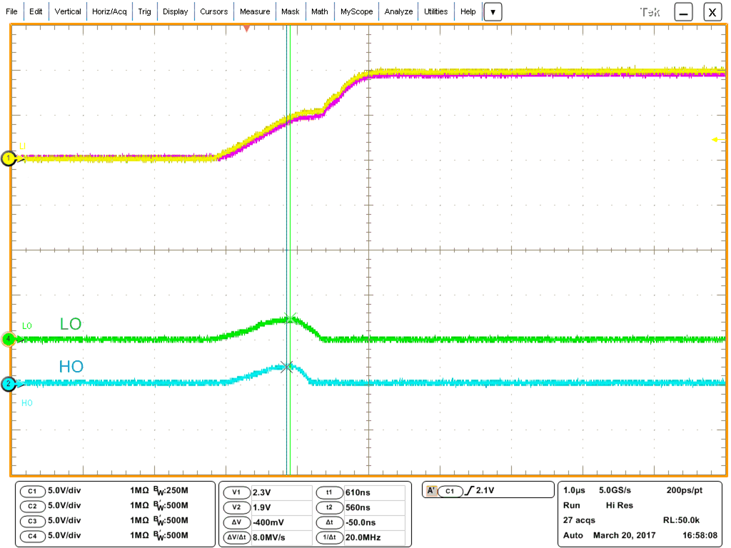 Figure 45. VDD/HB-HS Fast Ramp Up
9.2.2.4 Selecting Bootstrap Resistor (RBOOT)
Resistor RBOOT is selected to limit the current in DBOOT and limit the ramp up slew rate of voltage of HB-HS to avoid the phenomenon shown in Figure 45. It is recommended when using the UCC27712-Q1 that RBOOT is between 2 Ω and 20 Ω. For this design we selected an RBOOT current limiting resistor of 2.2 Ω. The bootstrap diode current (IDBOOT(pk)) was limited to roughly 5.0 A.

The power dissipation capability of the bootstrap resistor is important. The bootstrap resistor must be able to withstand the short period of high power dissipation during the initial charging sequence of the boot-strap capacitor. This energy is equivalent to 1/2 × CBOOT × V2. This energy is dissipated during the charging time of the bootstrap capacitor (~3 × RBOOT × CBOOT). Special attention must be paid to use a bigger size RBOOT when a bigger value of CBOOT is chosen.
9.2.2.5 Selecting Gate Resistor RON/ROFF
Resistor RON and ROFF are sized to achieve the following:
- Limit ringing caused by parasitic inductances and capacitances.
- Limit ringing caused by high voltage/current switching dV/dt, dI/dt, and body diode reverse recovery.
- Fine-tune gate drive strength to optimize switching loss.
- Reduce electromagnetic interference (EMI).
As mentioned in Output Stage, the UCC27712-Q1 has a pull up structure with a P-channel MOSFET providing a peak source current of 1.8A.
For this example 3.3-Ω resistors for RON and 2.2-Ω resistors for ROFF were selected to provide damping for ringing and ample gate drive current.

Therefore the peak source current can be predicted with:


where
- RON: External turn-on resistance
- RGFET_Int: Power transistor internal gate resistance, found in the power transistor datasheet.
- IO+ = Peak source current. The maximum values between 1.8 A, the UCC27712-Q1 peak source current, and the calculated value based on the gate drive loop resistance.
In this example:


Therefore, the high-side and low side peak source current is 1.6 A. Similarly, the peak sink current can be calculated with:


where
- ROFF: External turn-off resistance
- VDGATE: The diode forward voltage drop which is in series with ROFF. The diode in this example is an MBRM130L.
- IO- = Peak sink current. The maximum values between 2.8 A, the UCC27712-Q1 peak sink current, and the calculated value based on the gate drive loop resistance.
In this example:


9.2.2.6 Selecting Bootstrap Diode
A fast recovery diode should be chosen to avoid charge being taken away from the bootstrap capacitor. Thus, a fast reverse recovery time tRR, low forward voltage VF and low junction capacitance is recommended.
Suggested parts include MURA160T3G and BYG20J.
9.2.2.7 Estimate the UCC27712-Q1 Power Losses (PUCC27712-Q1)
The power losses of UCC27712-Q1 (PUCC27712-Q1) are estimated by calculating losses from several components. The gate drive loss in the UCC27712-Q1 is typically dominated by gate drive losses associated with charging and discharging the power device gate charge. There are other losses to consider especially if operating at high switching frequencies outlined below.
To determine the UCC27712-Q1 operating with no driver load, refer to the Typical Characteristics Figure 26 for IDD and IHB to determine the operating current at the appropriate fSW. The operating current power losses with no driver load are calculated in Equation 15:

Static losses due to leakage current (IBL) are calculated from the HB high-voltage node as shown in Equation 16:

Equation 17 calculates dynamic losses during the operation of the level shifter at HO turn-off edge. QP, typically 0.6 nC, is the charge absorbed by the level shifter during operation at each edge. Please note that if high-voltage switching occurs during HO turn-on as well (as in the case of ZVS topologies), then the power loss due to this component must be effectively doubled.

where
- VHV: DC link high voltage input in V
- fSW: Switching frequency of converter in Hz.
Dynamic losses incurred due to the gate charge while driving the FETs Q1 and Q2 are calculated Equation 18. Please note that this component typically dominates over the dynamic losses related to the internal VDD and VHB switching logic circuitry in UCC27712-Q1. The losses incurred driving the gate charge are not all dissipated in the gate driver device, this includes losses in the external gate resistance and internal power switch gate resistance.

The UCC27712-Q1 gate driver loss on the output stage ,PGDO, is part of PQG1,QG2. If the external gate resistances are zero most of the PQG1,QG2 will be dissipated in the UCC27712-Q1. If there are external gate resistances, the total loss will be distributed between the gate driver pull-up/down resistances and the external gate resistances.
The gate drive power dissipated within the UCC27712-Q1 driver can be determined by Equation 19:

In this example the gate drive related losses are approximately 60mW as shown in Equation 20:

For the conditions, VDD=12V, VHB = 400V, HO On-state Duty cycle D = 50%, QG = 68nC, fSW = 100kHz, the total power loss in UCC27712-Q1 driver for a half bridge power supply topology can be estimated as follows:

9.2.2.8 Estimating Junction Temperature
The junction temperature can be estimated with:

where
- TC is the UCC27712-Q1 case-top temperature measured with a thermocouple or some other instrument. and
- ѰJT is the junction-to-top characterization parameter from the Thermal Information table. Importantly.
Using the junction-to-top characterization parameter (ѰJT) instead of the junction-to-case thermal resistance (RθJC) can greatly improve the accuracy of estimating the junction temperature. The majority of the power dissipation of most devices is released into the PCB through the package leads, whereas only a small percentage of the total dissipation is released through the top of the case (where thermocouple measurements are usually taken). RθJC can only be used effectively when most of the thermal energy is released through the case, such as with metal packages or a heatsink is applied to the device package. In other cases RθJC will inaccurately estimate the true junction temperature of the device. ѰJT is experimentally derived by assuming the amount of thermal energy dissipated through the top of the device will be similar in both the testing environment and the application environment. As long as the recommended layout guidelines are observed, junction temperature can be estimated accurately to within a few degrees Celsius. For more information, see the Semiconductor and IC Package Thermal Metrics application report.
Additional Considerations: In the application example schematic there are 10-kΩ resistors across the gate and source terminals of FET Q1 and Q2. These resistors are placed across these nodes to ensure FETs Q1 and Q2 are not turned on if the UCC27712-Q1 is not in place or properly soldered to the circuit board or if UCC27712-Q1 is in an unbiased state.
9.2.2.9 Operation With IGBT's
The UCC27712-Q1 is well suited for driving IGBT's in various applications including motor drive and inverters. The design procedure is as the previous MOSFET example but the VDD voltage is typically 15-V to drive IGBT devices. Use the power transistor parameters and application specifications to determine the detail design and component values. See Figure 46 below for a typical IGBT application.
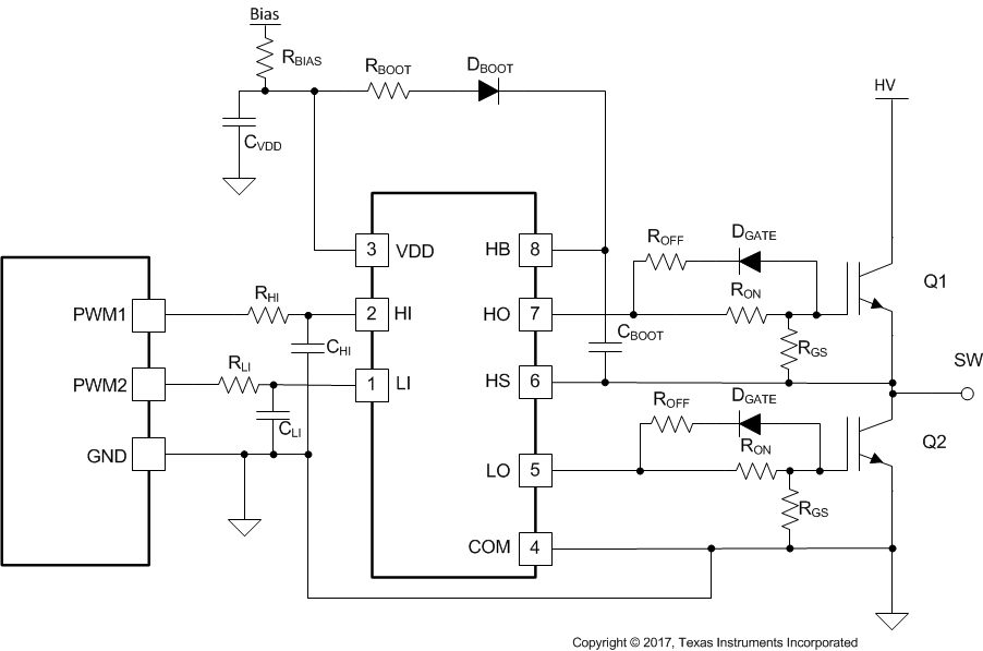 Figure 46. Typical IGBT Application Schematic
Refer to Figure 47 below for the UCC27712-Q1 driving 40-A, 650-V IGBT's in a high voltage sync buck configuration. The input voltage is 400 V, output 100 V with a 150-W output load. Channel 1 is the inductor current, Channel 2 is high-side IGBT VGE, Channel 3 is low-side IGBT VGE, and Channel 4 is the switch node or HS voltage.
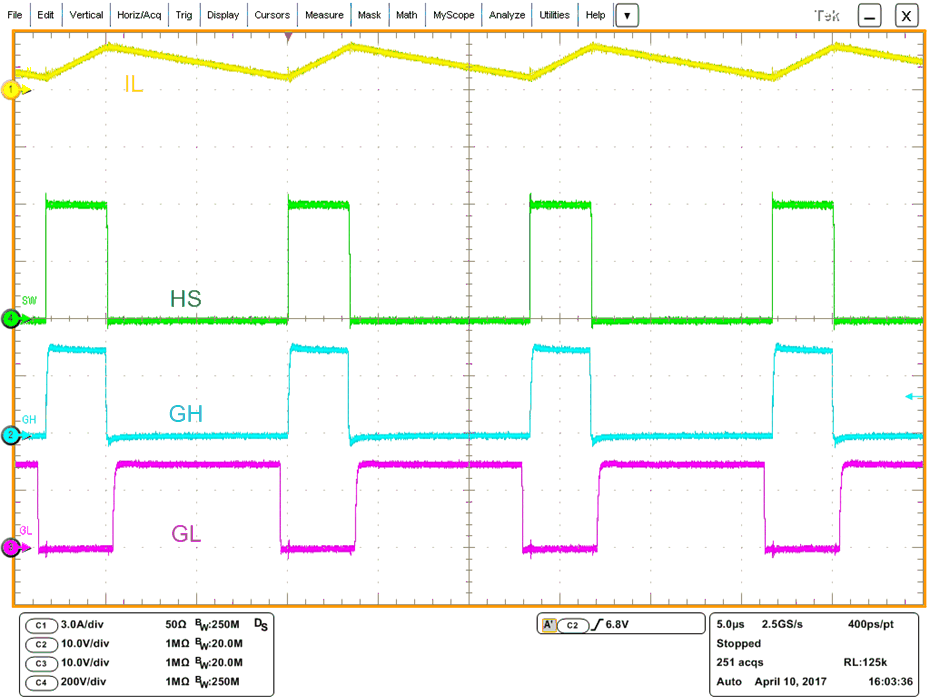 Figure 47. IGBT Sync-Buck Operating at 400 V and 150 W
9.2.3 Application Curves
Figure 48 and Figure 49 show the measured LI to LO turn-on and turn-off delay of one UCC27712-Q1 device. Channel 3 depicts LI and Channel 4 LO.
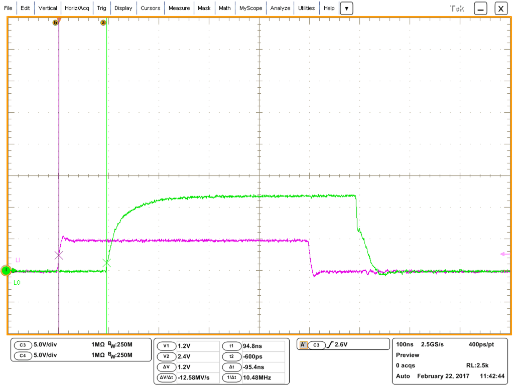 Figure 48. LI to LO Turn-On Propagation Delay
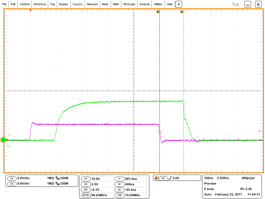 Figure 49. LI to LO Turn-Off Propagation Delay
Figure 50 and Figure 51 show the measured HI to HO turn-on and turn-off delay of one UCC27712-Q1 device. Channel 1 depicts HI and Channel 2 HO.
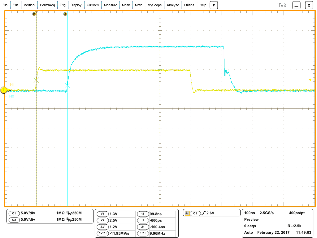 Figure 50. HI to HO Turn-On Propagation Delay
 Figure 52. MOSFET Sync-Buck Operating at 400 V and 150 W
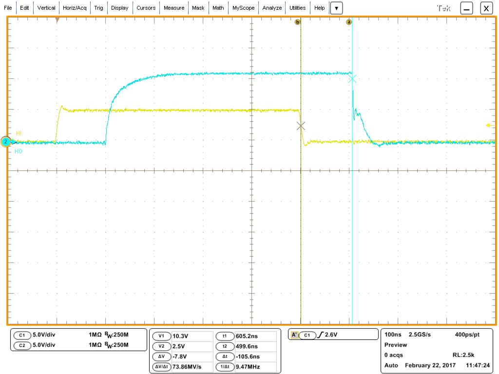 Figure 51. HI to HO Turn-Off Propagation Delay
Figure 52 shows UCC27712-Q1 operating in a high voltage sync-buck. Channel 1 depicts inductor current, Channel 2 high side MOSFET VGS, Channel 3 low side MOSFET VGS, and Channel 4 high voltage switch node.