SLUSAD3C June 2011 – October 2016
PRODUCTION DATA.
- 1 Features
- 2 Applications
- 3 Description
- 4 Revision History
- 5 Pin Configuration and Functions
- 6 Specifications
-
7 Detailed Description
- 7.1 Overview
- 7.2 Functional Block Diagram
- 7.3
Feature Description
- 7.3.1
Analog-to-Digital Conversion (ADC)
- 7.3.1.1 General Features
- 7.3.1.2 3-to-6 Series Cell Configuration
- 7.3.1.3 Cell Voltage Measurements
- 7.3.1.4 GPAI or VBAT Measurements
- 7.3.1.5 Temperature Measurement
- 7.3.1.6 ADC Band-Gap Voltage Reference
- 7.3.1.7 Conversion Control
- 7.3.1.8 Secondary Protection
- 7.3.1.9 Cell Overvoltage Fault Detection (COV)
- 7.3.1.10 Cell Undervoltage Fault Detection (CUV)
- 7.3.1.11 Overtemperature Detection
- 7.3.1.12 Fault and Alert Behavior
- 7.3.1.13 Secondary Protector Built-In Self-Test Features
- 7.3.2 Cell Balancing
- 7.3.3 Other Features and Functions
- 7.3.4 Communications
- 7.3.5 Device-to-Device Vertical Bus (VBUS) Interface
- 7.3.6 Packet Formats
- 7.3.7 Device Addressing
- 7.3.8 Changes and Enhancements for bq76PL536A
- 7.3.1
Analog-to-Digital Conversion (ADC)
- 7.4 Device Functional Modes
- 7.5 Programming
- 7.6
Register Maps
- 7.6.1 I/O Register Details
- 7.6.2 Register Types
- 7.6.3 Register Details
- 7.6.4 GPAI (0x01, 0x02) Register
- 7.6.5 VCELLn Register (0x03…0x0e)
- 7.6.6 TEMPERATURE1 Register (0x0f, 0x10)
- 7.6.7 TEMPERATURE2 Register (0x11, 0x12)
- 7.6.8 ALERT_STATUS Register (0x20)
- 7.6.9 FAULT_STATUS Register (0x21)
- 7.6.10 COV_FAULT Register (0x22)
- 7.6.11 CUV_FAULT Register (0x23)
- 7.6.12 PARITY_H Register (0x24) (PRESULT_A (R/O))
- 7.6.13 PARITY_H Register (0x25) (PRESULT_B (R/O))
- 7.6.14 ADC_CONTROL Register (0x30)
- 7.6.15 IO_CONTROL Register (0x31)
- 7.6.16 CB_CTRL Register (0x32)
- 7.6.17 CB_TIME Register (0x33)
- 7.6.18 ADC_CONVERT Register (0x34)
- 7.6.19 SHDW_CTRL Register (0x3a)
- 7.6.20 ADDRESS_CONTROL Register (0x3b)
- 7.6.21 RESET Register (0x3c)
- 7.6.22 TEST_SELECT Register (0x3d)
- 7.6.23 E_EN Register (0x3f)
- 7.6.24 FUNCTION_CONFIG Register (0x40)
- 7.6.25 IO_CONFIG Register (0x41)
- 7.6.26 CONFIG_COV Register (0x42)
- 7.6.27 CONFIG_COVT Register (0x43)
- 7.6.28 CONFIG_UV Register (0x44)
- 7.6.29 CONFIG_CUVT Register (0x45)
- 7.6.30 CONFIG_OT Register (0x46)
- 7.6.31 CONFIG_OTT Register (0x47)
- 7.6.32 USERx Register (0x48-0x4b) (USER1-4)
- 8 Application and Implementation
- 9 Power Supply Recommendations
- 10Layout
- 11Device and Documentation Support
- 12Mechanical, Packaging, and Orderable Information
Package Options
Mechanical Data (Package|Pins)
- PAP|64
Thermal pad, mechanical data (Package|Pins)
- PAP|64
Orderable Information
1 Features
- 3-to-6 Series Cell Support, All Chemistries
- Hot-Pluggable
- High-Speed Serial Peripheral Interface (SPI) for Data Communications
- Stackable Vertical Interface
- Isolation Components not Required Between Devices
- Industrial Temperature Range –40°C to 85°C
- High-Accuracy Analog-to-Digital Converter (ADC):
- ±1 mV Typical Accuracy
- 14-Bit Resolution, 6-µs Conversion Time
- Nine ADC Inputs: 6 Cell Voltages, 1 Six-Cell Brick Voltage, 2 Temperatures, 1 General-Purpose Input
- Dedicated Pins for Synchronizing Measurements
- Configuration Data Stored in Error Check/Correct (ECC)-One-Time-Programmable (OTP) Registers
- Built-In Comparators (Secondary Protector) for:
- Overvoltage and Undervoltage Protection
- Overtemperature Protection
- Programmable Thresholds and Delay Times
- Dedicated Fault Output Signals
- Cell Balancing Control Outputs With Safety Timeout
- Balance Current Set by External Components
- Supply Voltage Range from 6 V to 30 V Continuous and 36-V Peak
- Low Power:
- Typical 12-µA Sleep, 45-µA Idle
- Integrated Precision 5-V, 3-mA LDO
2 Applications
- Uninterruptible Power Systems (UPS)
- E-Bike and E-Scooter
- Large-Format Battery Systems
3 Description
The bq76PL536A device is a stackable battery monitor and protector for three-to-six lithium-ion cells in series. The bq76PL536A integrates an analog front end (AFE) along with a precision analog-to-digital converter (ADC), used to precisely measure battery cell voltages. A separate ADC is used to measure temperature.
In addition to temperature measurement, overvoltage and undervoltage are monitored per channel for protection. Non-volatile memory stores the user-programmable protection thresholds and delay times. A FAULT output signals whenever one of these thresholds is exceeded.
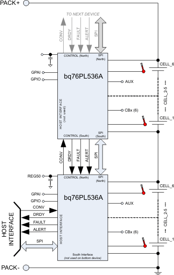
Cell stacks of 192 cells can be supported by stacked bq76PL536A devices. A high-speed SPI interface connects all devices.
Device Information(1)
| PART NUMBER | PACKAGE | BODY SIZE (NOM) |
|---|---|---|
| bq76PL536A | HTQFP (64) | 10.00 mm × 10.00 mm |
- For all available packages, see the orderable addendum at the end of the datasheet.
Simplified Schematic
