SBOS757 May 2016 TLV2369 , TLV369
PRODUCTION DATA.
- 1 Features
- 2 Applications
- 3 Description
- 4 Revision History
- 5 Pin Configuration and Functions
- 6 Specifications
- 7 Detailed Description
- 8 Application and Implementation
- 9 Power Supply Recommendations
- 10Layout
- 11Device and Documentation Support
- 12Mechanical, Packaging, and Orderable Information
Package Options
Mechanical Data (Package|Pins)
- DCK|5
Thermal pad, mechanical data (Package|Pins)
Orderable Information
1 Features
- Cost-Optimized Precision Amplifier nanoPower: 800 nA/Ch (Typ)
- Low Offset Voltage: 400 µV (Typ)
- Rail-to-Rail Input and Output
- Zero-Crossover Distortion
- Low Offset Drift: 0.5 µV/°C (Typ)
- Gain-Bandwidth Product: 12 kHz
- Supply Voltage: 1.8 V to 5.5 V
- microSize Packages: SC70-5, VSSOP-8
2 Applications
- Blood Glucose Meters
- Test Equipment
- Low-Power Sensor Signal Conditioning
- Portable Devices
3 Description
The TLV369 family of single and dual operational amplifiers represents a cost-optimized generation of 1.8-V nanopower amplifiers.
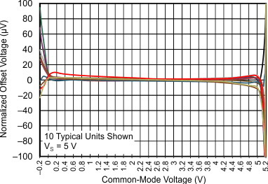
With the zero-crossover distortion circuitry, these amplifiers feature high linearity over the full common-mode input range with no crossover distortion, enabling true rail-to-rail input and operating from a 1.8-V to 5.5-V single supply. The family is also compatible with industry-standard nominal voltages of 3.0 V, 3.3 V, and 5.0 V.
The TLV369 (single version) is offered in a 5-pin SC70 package. The TLV2369 (dual version) comes in 8-pin VSSOP and SOIC packages.
Device Information(1)
| PART NUMBER | PACKAGE | BODY SIZE (NOM) |
|---|---|---|
| TLV369 | SC70 (5) | 2.00 mm × 1.25 mm |
| TLV2369 | VSSOP (8) | 3.00 mm × 3.00 mm |
| SOIC (8) | 4.90 mm × 3.91 mm |
- For all available packages, see the orderable addendum at the end of the data sheet.
TLV369 Family Eliminates Crossover Distortion
Across the Full Supply Range
