SBASAF6 October 2021 ADC09DJ1300 , ADC09QJ1300 , ADC09SJ1300
PRODUCTION DATA
- 1 Features
- 2 Applications
- 3 Description
- 4 Revision History
- 5 Description (continued)
- 6 Pin Configuration and Functions
-
7 Specifications
- 7.1 Absolute Maximum Ratings
- 7.2 ESD Ratings
- 7.3 Recommended Operating Conditions
- 7.4 Thermal Information
- 7.5 Electrical Characteristics: DC Specifications
- 7.6 Electrical Characteristics: Power Consumption
- 7.7 Electrical Characteristics: AC Specifications
- 7.8 Timing Requirements
- 7.9 Switching Characteristics
- 7.10 Typical Characteristics
-
8 Detailed Description
- 8.1 Overview
- 8.2 Functional Block Diagram
- 8.3
Feature Description
- 8.3.1 Device Comparison
- 8.3.2 Analog Input
- 8.3.3 ADC Core
- 8.3.4
Clocking
- 8.3.4.1 Converter PLL (C-PLL) for Sampling Clock Generation
- 8.3.4.2 LVDS Clock Outputs (PLLREFO±, TRIGOUT±)
- 8.3.4.3 Optional CMOS Clock Outputs (ORC, ORD)
- 8.3.4.4 SYSREF for JESD204C Subclass-1 Deterministic Latency
- 8.3.4.5
JESD204C Interface
- 8.3.4.5.1 Transport Layer
- 8.3.4.5.2 Scrambler
- 8.3.4.5.3 Link Layer
- 8.3.4.5.4 8B/10B Link Layer
- 8.3.4.5.5 64B/66B Link Layer
- 8.3.4.5.6 Physical Layer
- 8.3.4.5.7 JESD204C Enable
- 8.3.4.5.8 Multi-Device Synchronization and Deterministic Latency
- 8.3.4.5.9 Operation in Subclass 0 Systems
- 8.3.4.5.10 Alarm Monitoring
- 8.4
Device Functional Modes
- 8.4.1 Low Power Mode and High Performance Mode
- 8.4.2 JESD204C Modes
- 8.4.3 Power-Down Modes
- 8.4.4
Test Modes
- 8.4.4.1 Serializer Test-Mode Details
- 8.4.4.2 PRBS Test Modes
- 8.4.4.3 Clock Pattern Mode
- 8.4.4.4 Ramp Test Mode
- 8.4.4.5 Short and Long Transport Test Mode
- 8.4.4.6 D21.5 Test Mode
- 8.4.4.7 K28.5 Test Mode
- 8.4.4.8 Repeated ILA Test Mode
- 8.4.4.9 Modified RPAT Test Mode
- 8.4.4.10 Calibration Modes and Trimming
- 8.4.4.11 Offset Calibration
- 8.4.4.12 Trimming
- 8.5 Programming
- 8.6 SPI_Register_Map Registers
- 9 Application and Implementation
- 10Power Supply Recommendations
- 11Layout
- 12Device and Documentation Support
- 13Mechanical, Packaging, and Orderable Information
Package Options
Mechanical Data (Package|Pins)
- AAV|144
Thermal pad, mechanical data (Package|Pins)
Orderable Information
8.3.4 Clocking
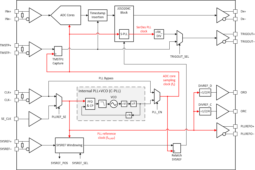
The input to the clocking subsystem of the device includes two clock inputs (CLK± and SE_CLK) and a synchronization signal (SYSREF±). An internal phase-locked loop (PLL) and voltage-controlled oscillator (VCO) can optionally be used to generate the ADC sampling clock from a low frequency reference by setting the PLL_EN pin high. The sampling clock PLL is called the converter PLL (C-PLL). The C-PLL reference can be provided to either the CLK± differential input or the SE_CLK single-ended input. The single-ended C-PLL reference input is selected by setting the PLLREF_SE pin high. For highest performance, the internal C-PLL can be bypassed and the sampling clock provided directly to the CLK± input when PLL_EN and PLLREF_SE are held low. Note that SE_CLK cannot be used if the C-PLL is disabled. The C-PLL reference clock can be sent to either an FPGA or ASIC or to an adjacent device through the PLLREFO± LVDS output when the PLL is enabled. Two additional copies or divided copies of PLLREFO can be output on ORC and ORD when enabled through the CLKCFG[1:0] pins or through SPI. PLLREFO and the ORC and ORD clock outputs are available at device power up when the CMOS control pins (PLL_EN, CLKCFG0 and CLKCFG1) are set appropriately and if PD is held low. Toggling PD high to power down the device also powers down the clock outputs.
In addition, the SerDes block contains a PLL, called S-PLL, that generates the SerDes output clock from the ADC sampling clock. The S-PLL generated clock can be divided and output from the TRIGOUT± LVDS output and sent to an FPGA or ASIC to clock the SerDes receivers. The SYSREF signal is captured by the chosen clock input (CLK± or SE_CLK). A SYSREF Windowing block is used to measure and optimize the setup and hold timing of the SYSREF signal relative to the selected clock input. SYSREF Windowing relaxes the timing requirement of the external signals. Figure 8-5 shows the clocking subsystem.
 Figure 8-5 Clocking Subsystem
The clock generated by the C-PLL when the PLL is enabled or the clock provided to CLK± when the PLL is disabled is used as the sampling clock for the ADC core as well as the clocking for the digital processing and serializer S-PLL. Use a low-noise (low jitter) clock input, whether the PLL is enabled or disabled, to maintain high signal-to-noise ratio (SNR) within the ADC.