SBAS997A February 2020 – June 2021 ADC09DJ1300-Q1 , ADC09QJ1300-Q1 , ADC09SJ1300-Q1
PRODUCTION DATA
- 1 Features
- 2 Applications
- 3 Description
- 4 Revision History
- 5 Description (continued)
- 6 Pin Configuration and Functions
-
7 Specifications
- 7.1 Absolute Maximum Ratings
- 7.2 ESD Ratings
- 7.3 Recommended Operating Conditions
- 7.4 Thermal Information
- 7.5 Electrical Characteristics: DC Specifications
- 7.6 Electrical Characteristics: Power Consumption
- 7.7 Electrical Characteristics: AC Specifications
- 7.8 Timing Requirements
- 7.9 Switching Characteristics
- 7.10 Typical Characteristics
-
8 Detailed Description
- 8.1 Overview
- 8.2 Functional Block Diagram
- 8.3
Feature Description
- 8.3.1 Device Comparison
- 8.3.2
Analog Input
- 8.3.2.1 Analog Input Protection
- 8.3.2.2 Full-Scale Voltage (VFS) Adjustment
- 8.3.2.3 Analog Input Offset Adjust
- 8.3.2.4 ADC Core
- 8.3.2.5 Temperature Monitoring Diode
- 8.3.2.6 Timestamp
- 8.3.2.7 Clocking
- 8.3.2.8
JESD204C Interface
- 8.3.2.8.1 Transport Layer
- 8.3.2.8.2 Scrambler
- 8.3.2.8.3 Link Layer
- 8.3.2.8.4 8B/10B Link Layer
- 8.3.2.8.5 64B/66B Link Layer
- 8.3.2.8.6 Physical Layer
- 8.3.2.8.7 JESD204C Enable
- 8.3.2.8.8 Multi-Device Synchronization and Deterministic Latency
- 8.3.2.8.9 Operation in Subclass 0 Systems
- 8.3.2.8.10 Alarm Monitoring
- 8.4
Device Functional Modes
- 8.4.1 Low Power Mode and High Performance Mode
- 8.4.2 JESD204C Modes
- 8.4.3 Power-Down Modes
- 8.4.4
Test Modes
- 8.4.4.1 Serializer Test-Mode Details
- 8.4.4.2 PRBS Test Modes
- 8.4.4.3 Clock Pattern Mode
- 8.4.4.4 Ramp Test Mode
- 8.4.4.5 Short and Long Transport Test Mode
- 8.4.4.6 D21.5 Test Mode
- 8.4.4.7 K28.5 Test Mode
- 8.4.4.8 Repeated ILA Test Mode
- 8.4.4.9 Modified RPAT Test Mode
- 8.4.4.10 Calibration Modes and Trimming
- 8.4.4.11 Offset Calibration
- 8.4.4.12 Trimming
- 8.5 Programming
- 8.6 SPI_Register_Map Registers
- 9 Application and Implementation
- 10Power Supply Recommendations
- 11Layout
- 12Device and Documentation Support
- 13Mechanical, Packaging, and Orderable Information
Package Options
Mechanical Data (Package|Pins)
- AAV|144
Thermal pad, mechanical data (Package|Pins)
Orderable Information
10 Power Supply Recommendations
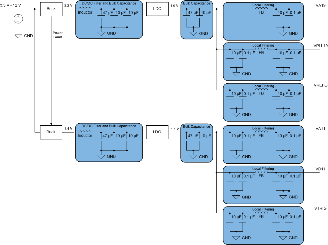
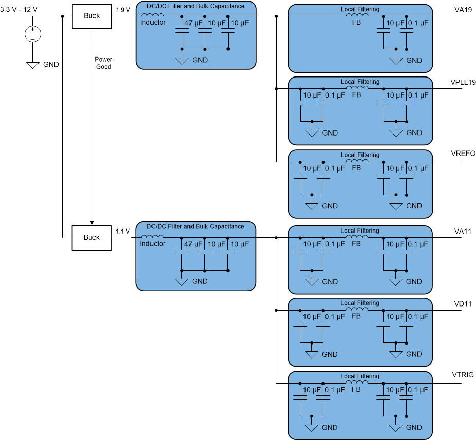
The device requires two different power-supply voltages. 1.9 V DC is required for the VA19, VPLL19 and VREFO power buses and 1.1 V DC is required for the VA11 and VD11 power buses. VTRIG can be set to either 1.1 V or 1.9 V and the TRIGOUT± common mode voltage shifts accordingly.
The power-supply voltages must be low noise and provide the needed current to achieve rated device performance. Certain supplies should be isolated from each other to prevent noise coupling into sensitive supplies. Isolation is best performed using separate regulators for each supply, but this is often not possible due to size and cost constraints. At a minimum a PI-type power supply filtering scheme should be used which includes a low-DC resistance ferrite bead (FB) with low-inductance decoupling capacitors on each side of the ferrite bead. These are demonstrated in the example power supply architectures drawings in Figure 10-1 and Figure 10-2.
There are two recommended power supply architectures:
- Step down using high-efficiency switching converters, followed by a second stage of regulation to provide switching noise reduction and improved voltage accuracy as shown in Figure 10-1.
- Directly step down the final ADC supply voltage using high-efficiency switching converters as shown in Figure 10-2. This approach provides the best efficiency, but care must be taken to ensure switching noise is minimized to prevent degraded ADC performance. In general, operate the DC/DC switching regulators in fixed-frequency mode at a high switching frequency to allow design of better power supply filtering networks and reduce low frequency noise that may not be able to be filtered.
The WEBENCH® Power Designer can be used to select and design the individual power supply elements as needed.
Recommended switching regulators include the TPS62290-Q1, TPS62812-Q1, TPS62065-Q1, TPS65268-Q1, and similar devices.
Recommended Low Drop-Out (LDO) linear regulators include the TPS74801-Q1, TPS7A88-Q1, TPS7A52-Q1 and similar devices.
For the switcher only approach, the ripple filter must be designed to provide sufficient filtering at the switching frequency of the DC-DC converter and harmonics of the switching frequency. Make a note of the switching frequency reported from WEBENCH® and design the EMI filter and capacitor combination to have the filter cutoff frequency set as needed. Each application has different tolerance for noise on the supply voltage and the impact to performance so strict ripple requirements are not provided. In general, the supply voltage must stay within the recommended operating conditions limits during all ripple and transient events. Any supply filtering must account for potential current transients, specifically when using low-power background calibration (see Low-Power Background Calibration (LPBG) Mode).

