SNAS825A December 2021 – April 2022 ADC128S102-SEP
PRODUCTION DATA
- 1 Features
- 2 Applications
- 3 Description
- 4 Revision History
- 5 Pin Configuration and Functions
- 6 Specifications
- 7 Detailed Description
- 8 Application and Implementation
- 9 Power Supply Recommendations
- 10Layout
- 11Device and Documentation Support
- 12Mechanical, Packaging, and Orderable Information
Package Options
Mechanical Data (Package|Pins)
- PW|16
Thermal pad, mechanical data (Package|Pins)
Orderable Information
9.2 Power Management
The ADC128S102-SEP is fully powered up when CS is low and is fully powered down when CS is high, with one exception. If operating in continuous conversion mode, the ADC128S102-SEP automatically enters power-down mode between the 16th SCLK falling edge of a conversion and the 1st SCLK falling edge of the subsequent conversion (see Figure 6-1).
In continuous conversion mode, the ADC128S102-SEP can perform multiple conversions back to back. Each conversion requires 16 SCLK cycles and the ADC128S102-SEP performs conversions continuously as long as CS is held low. Continuous mode offers maximum throughput.
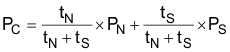
In burst mode, throughput can be traded off for power consumption by performing fewer conversions per unit time. In other words, more time is spent in power-down mode and less time is spent in normal mode. By using this technique, very low sample rates can be achieved while still using an SCLK frequency within the electrical specifications. To calculate the power consumption (PC), simply multiply the fraction of time spent in normal mode (tN) by the normal mode power consumption (PN), as shown in Equation 1, and add the fraction of time spent in shutdown mode (tS) multiplied by the shutdown mode power consumption (PS).