SBASA01B September   2020  – March 2022 ADC3660

PRODUCTION DATA  

  1. Features
  2. Applications
  3. Description
  4. Revision History
  5. Pin Configuration and Functions
  6. Specifications
    1. 6.1 Absolute Maximum Ratings
    2. 6.2 ESD Ratings
    3. 6.3 Recommended Operating Conditions
    4. 6.4 Thermal Information
    5. 6.5 Electrical Characteristics - Power Consumption
    6. 6.6 Electrical Characteristics - DC Specifications
    7. 6.7 Electrical Characteristics - AC Specifications
    8. 6.8 Timing Requirements
    9. 6.9 Typical Characteristics
  7. Parameter Measurement Information
  8. Detailed Description
    1. 8.1 Overview
    2. 8.2 Functional Block Diagram
    3. 8.3 Feature Description
      1. 8.3.1 Analog Input
        1. 8.3.1.1 Analog Input Bandwidth
        2. 8.3.1.2 Analog Front End Design
          1. 8.3.1.2.1 Sampling Glitch Filter Design
          2. 8.3.1.2.2 Analog Input Termination and DC Bias
            1. 8.3.1.2.2.1 AC-Coupling
            2. 8.3.1.2.2.2 DC-Coupling
        3. 8.3.1.3 Auto-Zero Feature
      2. 8.3.2 Clock Input
        1. 8.3.2.1 Single Ended vs Differential Clock Input
        2. 8.3.2.2 Signal Acquisition Time Adjust
      3. 8.3.3 Voltage Reference
        1. 8.3.3.1 Internal voltage reference
        2. 8.3.3.2 External voltage reference (VREF)
        3. 8.3.3.3 External voltage reference with internal buffer (REFBUF)
      4. 8.3.4 Digital Down Converter
        1. 8.3.4.1 DDC MUX
        2. 8.3.4.2 Digital Filter Operation
          1. 8.3.4.2.1 FS/4 Mixing with Real Output
        3. 8.3.4.3 Numerically Controlled Oscillator (NCO) and Digital Mixer
        4. 8.3.4.4 Decimation Filter
        5. 8.3.4.5 SYNC
        6. 8.3.4.6 Output Formatting with Decimation
      5. 8.3.5 Digital Interface
        1. 8.3.5.1 SDR Output Clocking
        2. 8.3.5.2 Output Data Format
        3. 8.3.5.3 Output Formatter
        4. 8.3.5.4 Output Bit Mapper
        5. 8.3.5.5 Output Interface/Mode Configuration
          1. 8.3.5.5.1 Configuration Example
      6. 8.3.6 Test Pattern
    4. 8.4 Device Functional Modes
      1. 8.4.1 Normal Operation
      2. 8.4.2 Power Down Options
      3. 8.4.3 Digital Channel Averaging
    5. 8.5 Programming
      1. 8.5.1 Configuration using PINs only
      2. 8.5.2 Configuration using the SPI interface
        1. 8.5.2.1 Register Write
        2. 8.5.2.2 Register Read
    6. 8.6 Register Maps
      1. 8.6.1 Detailed Register Description
  9. Application and Implementation
    1. 9.1 Typical Application
      1. 9.1.1 Design Requirements
      2. 9.1.2 Detailed Design Procedure
        1. 9.1.2.1 Input Signal Path
        2. 9.1.2.2 Sampling Clock
        3. 9.1.2.3 Voltage Reference
      3. 9.1.3 Application Curves
    2. 9.2 Initialization Set Up
      1. 9.2.1 Register Initialization During Operation
  10. 10Power Supply Recommendations
  11. 11Layout
    1. 11.1 Layout Guidelines
    2. 11.2 Layout Example
  12. 12Device and Documentation Support
    1. 12.1 Support Resources
    2. 12.2 Trademarks
    3. 12.3 Electrostatic Discharge Caution
    4. 12.4 Glossary
  13. 13Mechanical, Packaging, and Orderable Information

Package Options

Mechanical Data (Package|Pins)
Thermal pad, mechanical data (Package|Pins)
Orderable Information

Description

The ADC3660 device is a low-noise, ultra-low power, 16-bit, 65-MSPS dual-channel, high-speed analog-to-digital converter (ADCs). Designed for low power consumption, the device delivers a noise spectral density of –159 dBFS/Hz, combined with excellent linearity and dynamic range. The ADC3660 offers excellent dc precision, together with IF sampling support, which make the device an excellent choice for a wide range of applications. The ADC consumes only 71 mW/ch at 65 MSPS, and power consumption scales very well with lower sampling rates. In bypass mode (up to 31 MSPS) the output data is available after 1 or 2 clock cycles.

The ADC3660 uses a serial CMOS (SCMOS) interface to output the data which minimizes the number of digital interconnects. The device supports a two-lane, a one-lane and a half lane option. The serialized CMOS interface supports output rates to 250 Mbps which translates to ~ 15 MSPS (2-wire) to ~ 3.75 MSPS (0.5-wire) output rates after complex decimation. Hence the ADC3660 can be operated in 'oversampling + decimating' mode using the internal decimation filter in order to improve the dynamic range and relax external anti-aliasing filter.

The device comes in a 40-pin WQFN package (5 mm × 5 mm) and supports the extended industrial temperature range of –40 to +105⁰C.

Device Information
PART NUMBER (1)PACKAGEBODY SIZE (NOM)
ADC3660WQFN (40)5.00 × 5.00 mm
For all available packages, see the package option addendum at the end of the data sheet.
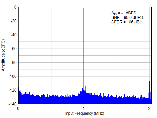
GUID-20200916-CA0I-7BGT-JT07-0QFDZDD16FBB-low.gif FS = 65 MSPS, Fin = 1 MHz, 16x Decimation, real