SBAS473E May   2009  – January 2018 ADS1013 , ADS1014 , ADS1015

PRODUCTION DATA.  

  1. Features
  2. Applications
  3. Description
    1.     Device Images
      1.      Simplified Block Diagrams
  4. Revision History
  5. Device Comparison Table
  6. Pin Configuration and Functions
    1.     Pin Functions
  7. Specifications
    1. 7.1 Absolute Maximum Ratings
    2. 7.2 ESD Ratings
    3. 7.3 Recommended Operating Conditions
    4. 7.4 Thermal Information
    5. 7.5 Electrical Characteristics
    6. 7.6 Timing Requirements: I2C
    7. 7.7 Typical Characteristics
  8. Detailed Description
    1. 8.1 Overview
    2. 8.2 Functional Block Diagrams
    3. 8.3 Feature Description
      1. 8.3.1 Multiplexer
      2. 8.3.2 Analog Inputs
      3. 8.3.3 Full-Scale Range (FSR) and LSB Size
      4. 8.3.4 Voltage Reference
      5. 8.3.5 Oscillator
      6. 8.3.6 Output Data Rate and Conversion Time
      7. 8.3.7 Digital Comparator (ADS1014 and ADS1015 Only)
      8. 8.3.8 Conversion Ready Pin (ADS1014 and ADS1015 Only)
      9. 8.3.9 SMbus Alert Response
    4. 8.4 Device Functional Modes
      1. 8.4.1 Reset and Power-Up
      2. 8.4.2 Operating Modes
        1. 8.4.2.1 Single-Shot Mode
        2. 8.4.2.2 Continuous-Conversion Mode
      3. 8.4.3 Duty Cycling For Low Power
    5. 8.5 Programming
      1. 8.5.1 I2C Interface
        1. 8.5.1.1 I2C Address Selection
        2. 8.5.1.2 I2C General Call
        3. 8.5.1.3 I2C Speed Modes
      2. 8.5.2 Slave Mode Operations
        1. 8.5.2.1 Receive Mode
        2. 8.5.2.2 Transmit Mode
      3. 8.5.3 Writing To and Reading From the Registers
      4. 8.5.4 Data Format
    6. 8.6 Register Map
      1. 8.6.1 Address Pointer Register (address = N/A) [reset = N/A]
        1. Table 4. Address Pointer Register Field Descriptions
      2. 8.6.2 Conversion Register (P[1:0] = 0h) [reset = 0000h]
        1. Table 5. Conversion Register Field Descriptions
      3. 8.6.3 Config Register (P[1:0] = 1h) [reset = 8583h]
        1. Table 6. Config Register Field Descriptions
      4. 8.6.4 Lo_thresh (P[1:0] = 2h) [reset = 8000h] and Hi_thresh (P[1:0] = 3h) [reset = 7FFFh] Registers
        1. Table 7. Lo_thresh and Hi_thresh Register Field Descriptions
  9. Application and Implementation
    1. 9.1 Application Information
      1. 9.1.1 Basic Connections
      2. 9.1.2 Single-Ended Inputs
      3. 9.1.3 Input Protection
      4. 9.1.4 Unused Inputs and Outputs
      5. 9.1.5 Analog Input Filtering
      6. 9.1.6 Connecting Multiple Devices
      7. 9.1.7 Quickstart Guide
    2. 9.2 Typical Application
      1. 9.2.1 Design Requirements
      2. 9.2.2 Detailed Design Procedure
        1. 9.2.2.1 Shunt Resistor Considerations
        2. 9.2.2.2 Operational Amplifier Considerations
        3. 9.2.2.3 ADC Input Common-Mode Considerations
        4. 9.2.2.4 Resistor (R1, R2, R3, R4) Considerations
        5. 9.2.2.5 Noise and Input Impedance Considerations
        6. 9.2.2.6 First-order RC Filter Considerations
        7. 9.2.2.7 Circuit Implementation
        8. 9.2.2.8 Results Summary
      3. 9.2.3 Application Curves
  10. 10Power Supply Recommendations
    1. 10.1 Power-Supply Sequencing
    2. 10.2 Power-Supply Decoupling
  11. 11Layout
    1. 11.1 Layout Guidelines
    2. 11.2 Layout Example
  12. 12Device and Documentation Support
    1. 12.1 Documentation Support
      1. 12.1.1 Related Documentation
    2. 12.2 Related Links
    3. 12.3 Receiving Notification of Documentation Updates
    4. 12.4 Community Resources
    5. 12.5 Trademarks
    6. 12.6 Electrostatic Discharge Caution
    7. 12.7 Glossary
  13. 13Mechanical, Packaging, and Orderable Information

Package Options

Mechanical Data (Package|Pins)
Thermal pad, mechanical data (Package|Pins)
Orderable Information

Multiplexer

The ADS1015 contains an input multiplexer (MUX), as shown in Figure 10. Either four single-ended or two differential signals can be measured. Additionally, AIN0 and AIN1 may be measured differentially to AIN3. The multiplexer is configured by bits MUX[2:0] in the Config register. When single-ended signals are measured, the negative input of the ADC is internally connected to GND by a switch within the multiplexer.
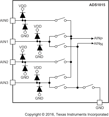
ADS1013 ADS1014 ADS1015 ai_fbd_mux_bas473.gifFigure 10. Input Multiplexer

The ADS1013 and ADS1014 do not have an input multiplexer and can measure either one differential signal or one single-ended signal. For single-ended measurements, connect the AIN1 pin to GND externally. In subsequent sections of this data sheet, AINP refers to AIN0 and AINN refers to AIN1 for the ADS1013 and ADS1014.

Electrostatic discharge (ESD) diodes connected to VDD and GND protect the ADS101x analog inputs. Keep the absolute voltage of any input within the range shown in Equation 1 to prevent the ESD diodes from turning on.

Equation 1. GND – 0.3 V < V(AINX) < VDD + 0.3 V

If the voltages on the input pins can potentially violate these conditions, use external Schottky diodes and series resistors to limit the input current to safe values (see the Absolute Maximum Ratings table).