SBASAH6A March 2022 – October 2022 ADS117L11
PRODUCTION DATA
- 1 Features
- 2 Applications
- 3 Description
- 4 Revision History
- 5 Pin Configuration and Functions
-
6 Specifications
- 6.1 Absolute Maximum Ratings
- 6.2 ESD Ratings
- 6.3 Recommended Operating Conditions
- 6.4 Thermal Information
- 6.5 Electrical Characteristics
- 6.6 Timing Requirements (1.65 V ≤ IOVDD ≤ 2 V)
- 6.7 Switching Characteristics (1.65 V ≤ IOVDD ≤ 2 V)
- 6.8 Timing Requirements (2 V < IOVDD ≤ 5.5 V)
- 6.9 Switching Characteristics (2 V < IOVDD ≤ 5.5 V)
- 6.10 Timing Diagrams
- 6.11 Typical Characteristics
- 7 Parameter Measurement Information
-
8 Detailed Description
- 8.1 Overview
- 8.2 Functional Block Diagram
- 8.3 Feature Description
- 8.4 Device Functional Modes
- 8.5 Programming
- 8.6
Registers
- 8.6.1 DEV_ID Register (Address = 0h) [reset = 01h]
- 8.6.2 REV_ID Register (Address = 1h) [reset = xxh]
- 8.6.3 STATUS Register (Address = 2h) [reset = x1100xxxb]
- 8.6.4 CONTROL Register (Address = 3h) [reset = 00h]
- 8.6.5 MUX Register (Address = 4h) [reset = 00h]
- 8.6.6 CONFIG1 Register (Address = 5h) [reset = 00h]
- 8.6.7 CONFIG2 Register (Address = 6h) [reset = 00h]
- 8.6.8 CONFIG3 Register (Address = 7h) [reset = 00h]
- 8.6.9 CONFIG4 Register (Address = 8h) [reset = 08h]
- 8.6.10 OFFSET2, OFFSET1, OFFSET0 Registers (Addresses = 9h, Ah, Bh) [reset = 00h, 00h, 00h]
- 8.6.11 GAIN2, GAIN1, GAIN0 Registers (Addresses = Ch, Dh, Eh) [reset = 40h, 00h, 00h]
- 8.6.12 CRC Register (Address = Fh) [reset = 00h]
- 9 Application and Implementation
- 10Device and Documentation Support
- 11Mechanical, Packaging, and Orderable Information
Package Options
Mechanical Data (Package|Pins)
- RUK|20
Thermal pad, mechanical data (Package|Pins)
- RUK|20
Orderable Information
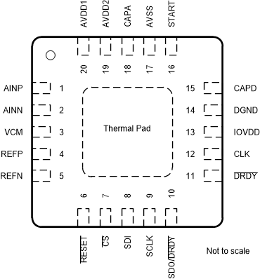
5 Pin Configuration and Functions
 Figure 5-1 RUK
Package,20-Pin WQFN(Top View)
Figure 5-1 RUK
Package,20-Pin WQFN(Top View)Table 5-1 Pin
Functions
| NAME | PIN NO. | I/O | DESCRIPTION |
|---|---|---|---|
| AINN | 2 | Analog input | Negative analog input; see the Analog Input section for details |
| AINP | 1 | Analog input | Positive analog input; see the Analog Input section for details |
| AVDD1 | 20 | Analog Supply | Positive analog supply 1; see the Section 8.3.6 section for details |
| AVDD2 | 19 | Analog Supply | Positive analog supply 2; see the Section 8.3.6 section for details |
| AVSS | 17 | Analog Supply | Negative analog supply; see the Section 8.3.6 section for details |
| CAPA | 18 | Analog output | Analog voltage regulator output capacitor bypass |
| CAPD | 15 | Analog output | Digital voltage regulator output capacitor bypass |
| CLK | 12 | Digital input | Clock input; see the Section 8.3.3 section for details |
| CS | 7 | Digital input | Chip select, active low; see the Chip Select section for details |
| DGND | 14 | Ground | Digital ground |
| DRDY | 11 | Digital output | Data ready, active low; see the Section 8.5.7.2 section for details |
| IOVDD | 13 | Digital Supply | I/O supply voltage; see the Section 8.3.6 section for details |
| REFN | 5 | Analog input | Negative reference input; see the Reference Voltage section for details |
| REFP | 4 | Analog input | Positive reference input; see the Reference Voltage section for details |
| RESET | 6 | Digital input | Reset, active low; see the Section 8.4.5 section for details |
| SCLK | 9 | Digital input | Serial data clock; see the Serial Clock section for details |
| SDI | 8 | Digital input | Serial data input; see the Serial Data Input section for details |
| SDO/DRDY | 10 | Digital output | Serial data output and data ready (optional); see the SDO/DRDY section for details |
| START | 16 | Digital input | Conversion start; see the Section 8.4.6 section for details |
| VCM | 3 | Analog output | Common-mode voltage buffered output; see the Section 8.3.7 section for details |
| Thermal Pad | Pad | — | Thermal power pad; connect to AVSS |