SBAS350G June 2005 – January 2021 ADS1232 , ADS1234
PRODUCTION DATA
- 1 Features
- 2 Applications
- 3 Description
- 4 Revision History
- 5 Pin Configuration and Functions
- 6 Specifications
- 7 Parameter Measurement Information
-
8 Detailed Description
- 8.1 Overview
- 8.2 Functional Block Diagram
- 8.3
Feature Description
- 8.3.1 Analog Inputs (AINPX, AINNX)
- 8.3.2 Temperature Sensor (ADS1232 Only)
- 8.3.3 Low-Noise PGA
- 8.3.4 Voltage Reference Inputs (REFP, REFN)
- 8.3.5 Clock Sources
- 8.3.6 Digital Filter Frequency Response
- 8.3.7 Settling Time
- 8.3.8 Data Rate
- 8.3.9 Data Format
- 8.3.10 Data Ready and Data Output (DRDY/DOUT)
- 8.3.11 Serial Clock Input (SCLK)
- 8.3.12 Data Retrieval
- 8.4 Device Functional Modes
- 9 Application and Implementation
- 10Power Supply Recommendations
- 11Layout
- 12Device and Documentation Support
- 13Mechanical, Packaging, and Orderable Information
Package Options
Mechanical Data (Package|Pins)
- PW|24
Thermal pad, mechanical data (Package|Pins)
- PW|24
Orderable Information
8.3.3 Low-Noise PGA
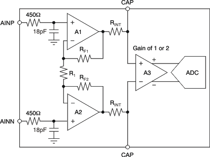
The ADS123x feature a low-drift, low-noise PGA that provides a complete front-end solution for bridge sensors. A simplified diagram of the PGA is shown in Figure 8-2. The PGA consists of two chopper-stabilized amplifiers (A1 and A2) and three accurately matched resistors (R1, RF1, and RF2), which construct a differential front-end stage with a gain of 64, followed by gain stage A3. The PGA inputs are equipped with an EMI filter, as shown in Figure 8-2. The cut-off frequency of the EMI filter is 19.6 MHz. If the PGA gain is set to 1 or 2, the gain-of-64 stage is bypassed and shut down to save power. With the combination of both gain stages, the PGA gain can be set to 64 or 128. The PGA gain of the ADS123x is set to 1, 2, 64, or 128 by pins GAIN1 (MSB) and GAIN0 (LSB). Table 8-3 shows the gain setting of the PGA.
| GAIN[1:0] INPUT PINS | PGA GAIN |
|---|---|
| 00 | 1 |
| 01 | 2 |
| 10 | 64 |
| 11 | 128 |
By using AVDD as the reference input, the bipolar input ranges from ±2.5 V to ±19.5 mV, while the unipolar ranges from 2.5 V to 19.5 mV. When the PGA gain is set to 1 or 2, the absolute inputs can go rail-to-rail without significant performance degradation. However, the inputs of the ADS123x are protected with internal diodes connected to the power-supply rails. These diodes clamp the applied signal to prevent damage to the input circuitry. On the other hand, when the PGA gain is set to 64 or 128, the operating input range is limited to (AGND + 1.5 V) to (AVDD – 1.5 V), in order to prevent saturating the differential front-end circuitry and degrading performance.
 Figure 8-2 Simplified Diagram of the PGA