SBAS661C February 2015 – May 2021 ADS1262 , ADS1263
PRODUCTION DATA
- 1 Features
- 2 Applications
- 3 Description
- 4 Revision History
- 5 Device Comparison
- 6 Pin Configuration and Functions
- 7 Specifications
-
8 Parameter Measurement Information
- 8.1 Offset Temperature Drift Measurement
- 8.2 Gain Temperature Drift Measurement
- 8.3 Common-Mode Rejection Ratio Measurement
- 8.4 Power-Supply Rejection Ratio Measurement
- 8.5 Crosstalk Measurement (ADS1263)
- 8.6 Reference-Voltage Temperature-Drift Measurement
- 8.7 Reference-Voltage Thermal-Hysteresis Measurement
- 8.8 Noise Performance
-
9 Detailed Description
- 9.1 Overview
- 9.2 Functional Block Diagram
- 9.3
Feature Description
- 9.3.1 Multifunction Analog Inputs
- 9.3.2 Analog Input Description
- 9.3.3 Sensor Bias
- 9.3.4 Temperature Sensor
- 9.3.5 Power-Supply Monitor
- 9.3.6 PGA
- 9.3.7 PGA Voltage Overrange Monitors
- 9.3.8 ADC Reference Voltage
- 9.3.9 ADC1 Modulator
- 9.3.10 Digital Filter
- 9.3.11 Sensor-Excitation Current Sources (IDAC1 and IDAC2)
- 9.3.12 Level-Shift Voltage
- 9.3.13 General-Purpose Input/Output (GPIO)
- 9.3.14 Test DAC (TDAC)
- 9.3.15 ADC2 (ADS1263)
- 9.4
Device Functional Modes
- 9.4.1 Conversion Control
- 9.4.2 Conversion Latency
- 9.4.3 Programmable Time Delay
- 9.4.4 Serial Interface
- 9.4.5 Data Ready Pin (DRDY)
- 9.4.6 Conversion Data Software Polling
- 9.4.7 Read Conversion Data
- 9.4.8 ADC Clock Modes
- 9.4.9
Calibration
- 9.4.9.1 Offset and Full-Scale Calibration
- 9.4.9.2 ADC1 Offset Self-Calibration (SFOCAL1)
- 9.4.9.3 ADC1 Offset System Calibration (SYOCAL1)
- 9.4.9.4 ADC2 Offset Self-Calibration ADC2 (SFOCAL2)
- 9.4.9.5 ADC2 Offset System Calibration ADC2 (SYOCAL2)
- 9.4.9.6 ADC1 Full-Scale System Calibration (SYGCAL1)
- 9.4.9.7 ADC2 Full-Scale System Calibration ADC2 (SYGCAL2)
- 9.4.9.8 Calibration Command Procedure
- 9.4.9.9 User Calibration Procedure
- 9.4.10 Reset
- 9.4.11 Power-Down Mode
- 9.4.12 Chop Mode
- 9.5 Programming
- 9.6
Register Maps
- 9.6.1 Device Identification Register (address = 00h) [reset = x]
- 9.6.2 Power Register (address = 01h) [reset = 11h]
- 9.6.3 Interface Register (address = 02h) [reset = 05h]
- 9.6.4 Mode0 Register (address = 03h) [reset = 00h]
- 9.6.5 Mode1 Register (address = 04h) [reset = 80h]
- 9.6.6 Mode2 Register (address = 05h) [reset = 04h]
- 9.6.7 Input Multiplexer Register (address = 06h) [reset = 01h]
- 9.6.8 Offset Calibration Registers (address = 07h, 08h, 09h) [reset = 00h, 00h, 00h]
- 9.6.9 Full-Scale Calibration Registers (address = 0Ah, 0Bh, 0Ch) [reset = 40h, 00h, 00h]
- 9.6.10 IDACMUX Register (address = 0Dh) [reset = BBh]
- 9.6.11 IDACMAG Register (address = 0Eh) [reset = 00h]
- 9.6.12 REFMUX Register (address = 0Fh) [reset = 00h]
- 9.6.13 TDACP Control Register (address = 10h) [reset = 00h]
- 9.6.14 TDACN Control Register (address = 11h) [reset = 00h]
- 9.6.15 GPIO Connection Register (address = 12h) [reset = 00h]
- 9.6.16 GPIO Direction Register (address = 13h) [reset = 00h]
- 9.6.17 GPIO Data Register (address = 14h) [reset = 00h]
- 9.6.18 ADC2 Configuration Register (address = 15h) [reset = 00h]
- 9.6.19 ADC2 Input Multiplexer Register (address = 16h) [reset = 01h]
- 9.6.20 ADC2 Offset Calibration Registers (address = 17h, 18h) [reset = 00h, 00h]
- 9.6.21 ADC2 Full-Scale Calibration Registers (address = 19h, 1Ah) [reset = 00h, 40h]
- 10Application and Implementation
- 11Power Supply Recommendations
- 12Layout
- 13Device and Documentation Support
Package Options
Mechanical Data (Package|Pins)
- PW|28
Thermal pad, mechanical data (Package|Pins)
- PW|28
Orderable Information
9.4.1 Conversion Control
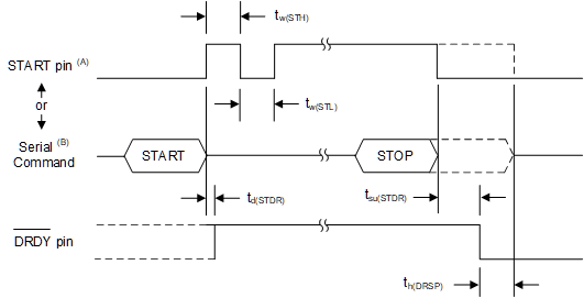
ADC1 conversions are controlled by the START pin or by serial commands. If using commands to control ADC1 conversions, keep the START pin low to avoid possible contentions between the START pin and commands.
ADC1 has two conversion modes: continuous or pulse. Continuous-conversion mode converts indefinitely until stopped by the user. Pulse-conversion mode performs one conversion after the START pin is taken high or after the start command is sent. Use RUNMODE (bit 6, MODE0) to program the conversion mode. Figure 9-38 shows the start and stop timing to control ADC conversions.

START and
DRDY pins apply only to ADC1 operation.
Start and stop opcodes take effect on the 7th SCLK falling edge.
Start and stop opcodes:
Figure 9-38 ADC1 Start and Stop Conversion Timing- START1 for ADC1: 08h or 09h
- START2 for ADC2: 0Ch or 0Dh
- STOP1 for ADC1: 0Ah or 0Bh
- STOP2 for ADC2: 0Eh or 0Fh
Table 9-12 ADC1 START and STOP Conversion Timing
Requirements
| PARAMETER | TEST CONDITIONS | MIN | MAX | UNIT | |
|---|---|---|---|---|---|
| tw(STH) | START pin high: pulse duration | 4 | tCLK(1) | ||
| tw(STL) | START pin low to re-start conversion: pulse duration | 4 | tCLK | ||
| td(STDR) | Start condition to DRDY high: delay time | Pulse conversion mode | 2 | tCLK | |
| tsu(STDR) | Stop condition to DRDY↓ stopping additional conversions: set-up time | Continuous conversion mode | 16 | tCLK | |
| th(DRSP) | DRDY↓ to stop condition to continue current conversion: hold time | Continuous conversion mode | 16 | tCLK | |
(1) tCLK = 1 / fCLK