SBAS661C February 2015 – May 2021 ADS1262 , ADS1263
PRODUCTION DATA
- 1 Features
- 2 Applications
- 3 Description
- 4 Revision History
- 5 Device Comparison
- 6 Pin Configuration and Functions
- 7 Specifications
-
8 Parameter Measurement Information
- 8.1 Offset Temperature Drift Measurement
- 8.2 Gain Temperature Drift Measurement
- 8.3 Common-Mode Rejection Ratio Measurement
- 8.4 Power-Supply Rejection Ratio Measurement
- 8.5 Crosstalk Measurement (ADS1263)
- 8.6 Reference-Voltage Temperature-Drift Measurement
- 8.7 Reference-Voltage Thermal-Hysteresis Measurement
- 8.8 Noise Performance
-
9 Detailed Description
- 9.1 Overview
- 9.2 Functional Block Diagram
- 9.3
Feature Description
- 9.3.1 Multifunction Analog Inputs
- 9.3.2 Analog Input Description
- 9.3.3 Sensor Bias
- 9.3.4 Temperature Sensor
- 9.3.5 Power-Supply Monitor
- 9.3.6 PGA
- 9.3.7 PGA Voltage Overrange Monitors
- 9.3.8 ADC Reference Voltage
- 9.3.9 ADC1 Modulator
- 9.3.10 Digital Filter
- 9.3.11 Sensor-Excitation Current Sources (IDAC1 and IDAC2)
- 9.3.12 Level-Shift Voltage
- 9.3.13 General-Purpose Input/Output (GPIO)
- 9.3.14 Test DAC (TDAC)
- 9.3.15 ADC2 (ADS1263)
- 9.4
Device Functional Modes
- 9.4.1 Conversion Control
- 9.4.2 Conversion Latency
- 9.4.3 Programmable Time Delay
- 9.4.4 Serial Interface
- 9.4.5 Data Ready Pin (DRDY)
- 9.4.6 Conversion Data Software Polling
- 9.4.7 Read Conversion Data
- 9.4.8 ADC Clock Modes
- 9.4.9
Calibration
- 9.4.9.1 Offset and Full-Scale Calibration
- 9.4.9.2 ADC1 Offset Self-Calibration (SFOCAL1)
- 9.4.9.3 ADC1 Offset System Calibration (SYOCAL1)
- 9.4.9.4 ADC2 Offset Self-Calibration ADC2 (SFOCAL2)
- 9.4.9.5 ADC2 Offset System Calibration ADC2 (SYOCAL2)
- 9.4.9.6 ADC1 Full-Scale System Calibration (SYGCAL1)
- 9.4.9.7 ADC2 Full-Scale System Calibration ADC2 (SYGCAL2)
- 9.4.9.8 Calibration Command Procedure
- 9.4.9.9 User Calibration Procedure
- 9.4.10 Reset
- 9.4.11 Power-Down Mode
- 9.4.12 Chop Mode
- 9.5 Programming
- 9.6
Register Maps
- 9.6.1 Device Identification Register (address = 00h) [reset = x]
- 9.6.2 Power Register (address = 01h) [reset = 11h]
- 9.6.3 Interface Register (address = 02h) [reset = 05h]
- 9.6.4 Mode0 Register (address = 03h) [reset = 00h]
- 9.6.5 Mode1 Register (address = 04h) [reset = 80h]
- 9.6.6 Mode2 Register (address = 05h) [reset = 04h]
- 9.6.7 Input Multiplexer Register (address = 06h) [reset = 01h]
- 9.6.8 Offset Calibration Registers (address = 07h, 08h, 09h) [reset = 00h, 00h, 00h]
- 9.6.9 Full-Scale Calibration Registers (address = 0Ah, 0Bh, 0Ch) [reset = 40h, 00h, 00h]
- 9.6.10 IDACMUX Register (address = 0Dh) [reset = BBh]
- 9.6.11 IDACMAG Register (address = 0Eh) [reset = 00h]
- 9.6.12 REFMUX Register (address = 0Fh) [reset = 00h]
- 9.6.13 TDACP Control Register (address = 10h) [reset = 00h]
- 9.6.14 TDACN Control Register (address = 11h) [reset = 00h]
- 9.6.15 GPIO Connection Register (address = 12h) [reset = 00h]
- 9.6.16 GPIO Direction Register (address = 13h) [reset = 00h]
- 9.6.17 GPIO Data Register (address = 14h) [reset = 00h]
- 9.6.18 ADC2 Configuration Register (address = 15h) [reset = 00h]
- 9.6.19 ADC2 Input Multiplexer Register (address = 16h) [reset = 01h]
- 9.6.20 ADC2 Offset Calibration Registers (address = 17h, 18h) [reset = 00h, 00h]
- 9.6.21 ADC2 Full-Scale Calibration Registers (address = 19h, 1Ah) [reset = 00h, 40h]
- 10Application and Implementation
- 11Power Supply Recommendations
- 12Layout
- 13Device and Documentation Support
Package Options
Mechanical Data (Package|Pins)
- PW|28
Thermal pad, mechanical data (Package|Pins)
- PW|28
Orderable Information
9.3.15.5 ADC2 Digital Filter
The ADC2 digital filter receives the modulator output and produces a 24-bit digital output. The digital filter low-pass filters and down-samples the modulator data to yield the final data rate. The ADC2 digital filter is a cascade of two stages. The first stage is a sinc3 filter that decimates by 64, 128, or 512, to derive data rates of 800 SPS, 400 SPS, or 100 SPS, respectively. The second stage receives the output of the first stage at 100 SPS. The second stage is a sinc1 filter with decimation equal to ten that derives the data rate of 10 SPS, as illustrated in Figure 9-31. The ADC bypasses the second stage for data rates of 800 SPS, 400 SPS, and 100 SPS. Table 9-10 shows the sinc filter data rates and decimation ratios (A and B) that correspond to each filter stage. The overall filter decimation ratio is the product of A and B decimation ratios. The data rate is programmed by the DR2[1:0] bits of register ADC2CFG.
 Figure 9-31 ADC2 Digital Filter Block Diagram
| DATA RATE (SPS)(1) | DR2[1:0] BITS OF REGISTER ADC2CFG | 1st STAGE DECIMATION RATIO A | 2nd STAGE DECIMATION RATIO B |
|---|---|---|---|
| 10 ( default) | 00 | 512 | 10 |
| 100 | 01 | 512 | - |
| 400 | 10 | 128 | - |
| 800 | 11 | 64 | - |
The low pass nature of the ADC2 sinc filter establishes the overall frequency response. The frequency response is given by Equation 17:
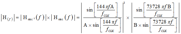
where
- f = Input frequency
- fCLK = ADC clock (7.3728 MHz)
- A = First stage decimation ratio
- B = Second stage decimation ratio
Figures Figure 9-32 through Figure 9-36 show the frequency response of different ADC2 data rates. Nulls are located in the frequency response at the data rate and at data rate multiples. Figure 9-32 (data rate = 10 SPS) has frequency response nulls at 50 Hz and 60 Hz and their multiples. Therefore, the rate of 10 SPS provides rejection of power line cycle frequencies. Figure 9-33 shows filter response detail of frequencies centered around 50 Hz and 60 Hz.
 Figure 9-32 ADC2 10 SPS Frequency Response
 Figure 9-34 ADC2 100 SPS Frequency Response
 Figure 9-36 ADC2 800 SPS Frequency Response
 Figure 9-33 ADC2 10 SPS Frequency Response 50-Hz and 60-Hz Detail
 Figure 9-35 ADC2 400 SPS Frequency Response
Table 9-11 summarizes the ADC2 digital filter –3-dB bandwidth and 50-Hz and 60-Hz line-cycle rejection based on 2% and 6% ratio tolerance of power-line frequency to ADC clock frequency. The sample rate of 10 SPS has frequency response nulls at 50 Hz and 60 Hz; therefore, this data rate provides the best possible rejection of power-line interference.
| DATA RATE (SPS) | -3-dB BANDWIDTH (Hz) | DIGITAL FILTER RESPONSE (dB) | |||
|---|---|---|---|---|---|
| 50-Hz REJECTION ±2% | 60-Hz REJECTION ±2% | 50-Hz REJECTION ±6% | 60-Hz REJECTION ±6% | ||
| 10 | 4.4 | –41 | –47 | –32 | –36 |
| 100 | 26 | –12 | –17 | –10 | –16 |
| 400 | 104 | –0.5 | –0.9 | –0.5 | –0.9 |
| 800 | 208 | –0.2 | –0.2 | –0.1 | –0.2 |
The ADC digital filter provides attenuation of frequencies greater than ½ of the data rate (Nyquist frequency) to minimize out-of-band frequencies folding back to the bandwidth of interest. As with all digital filters, response images appear at frequency multiples of the filter input frequency (fMOD2 = fCLK / 144 = 51.2 kHz). Figure 9-37 shows the frequency response to 175 kHz for DR = 800 SPS. The response near dc is the desired signal bandwidth. Note how the filter response repeats at multiplies of 51.2 kHz. The filter response repeats at frequencies shown in Equation 18:
where
- N = 1, 2, 3...
- fDR2 = ADC2 data-rate frequency
The digital filter attenuates signal or noise up to the frequency where the response repeats. However, any signal or noise present within the frequency bands where the response repeats aliases into the passband, unless attenuated by an analog filter. Often, using a simple RC analog filter is sufficient to reject these frequencies.
 Figure 9-37 ADC2 Frequency Response to 175 kHz