SBAS661C February 2015 – May 2021 ADS1262 , ADS1263
PRODUCTION DATA
- 1 Features
- 2 Applications
- 3 Description
- 4 Revision History
- 5 Device Comparison
- 6 Pin Configuration and Functions
- 7 Specifications
-
8 Parameter Measurement Information
- 8.1 Offset Temperature Drift Measurement
- 8.2 Gain Temperature Drift Measurement
- 8.3 Common-Mode Rejection Ratio Measurement
- 8.4 Power-Supply Rejection Ratio Measurement
- 8.5 Crosstalk Measurement (ADS1263)
- 8.6 Reference-Voltage Temperature-Drift Measurement
- 8.7 Reference-Voltage Thermal-Hysteresis Measurement
- 8.8 Noise Performance
-
9 Detailed Description
- 9.1 Overview
- 9.2 Functional Block Diagram
- 9.3
Feature Description
- 9.3.1 Multifunction Analog Inputs
- 9.3.2 Analog Input Description
- 9.3.3 Sensor Bias
- 9.3.4 Temperature Sensor
- 9.3.5 Power-Supply Monitor
- 9.3.6 PGA
- 9.3.7 PGA Voltage Overrange Monitors
- 9.3.8 ADC Reference Voltage
- 9.3.9 ADC1 Modulator
- 9.3.10 Digital Filter
- 9.3.11 Sensor-Excitation Current Sources (IDAC1 and IDAC2)
- 9.3.12 Level-Shift Voltage
- 9.3.13 General-Purpose Input/Output (GPIO)
- 9.3.14 Test DAC (TDAC)
- 9.3.15 ADC2 (ADS1263)
- 9.4
Device Functional Modes
- 9.4.1 Conversion Control
- 9.4.2 Conversion Latency
- 9.4.3 Programmable Time Delay
- 9.4.4 Serial Interface
- 9.4.5 Data Ready Pin (DRDY)
- 9.4.6 Conversion Data Software Polling
- 9.4.7 Read Conversion Data
- 9.4.8 ADC Clock Modes
- 9.4.9
Calibration
- 9.4.9.1 Offset and Full-Scale Calibration
- 9.4.9.2 ADC1 Offset Self-Calibration (SFOCAL1)
- 9.4.9.3 ADC1 Offset System Calibration (SYOCAL1)
- 9.4.9.4 ADC2 Offset Self-Calibration ADC2 (SFOCAL2)
- 9.4.9.5 ADC2 Offset System Calibration ADC2 (SYOCAL2)
- 9.4.9.6 ADC1 Full-Scale System Calibration (SYGCAL1)
- 9.4.9.7 ADC2 Full-Scale System Calibration ADC2 (SYGCAL2)
- 9.4.9.8 Calibration Command Procedure
- 9.4.9.9 User Calibration Procedure
- 9.4.10 Reset
- 9.4.11 Power-Down Mode
- 9.4.12 Chop Mode
- 9.5 Programming
- 9.6
Register Maps
- 9.6.1 Device Identification Register (address = 00h) [reset = x]
- 9.6.2 Power Register (address = 01h) [reset = 11h]
- 9.6.3 Interface Register (address = 02h) [reset = 05h]
- 9.6.4 Mode0 Register (address = 03h) [reset = 00h]
- 9.6.5 Mode1 Register (address = 04h) [reset = 80h]
- 9.6.6 Mode2 Register (address = 05h) [reset = 04h]
- 9.6.7 Input Multiplexer Register (address = 06h) [reset = 01h]
- 9.6.8 Offset Calibration Registers (address = 07h, 08h, 09h) [reset = 00h, 00h, 00h]
- 9.6.9 Full-Scale Calibration Registers (address = 0Ah, 0Bh, 0Ch) [reset = 40h, 00h, 00h]
- 9.6.10 IDACMUX Register (address = 0Dh) [reset = BBh]
- 9.6.11 IDACMAG Register (address = 0Eh) [reset = 00h]
- 9.6.12 REFMUX Register (address = 0Fh) [reset = 00h]
- 9.6.13 TDACP Control Register (address = 10h) [reset = 00h]
- 9.6.14 TDACN Control Register (address = 11h) [reset = 00h]
- 9.6.15 GPIO Connection Register (address = 12h) [reset = 00h]
- 9.6.16 GPIO Direction Register (address = 13h) [reset = 00h]
- 9.6.17 GPIO Data Register (address = 14h) [reset = 00h]
- 9.6.18 ADC2 Configuration Register (address = 15h) [reset = 00h]
- 9.6.19 ADC2 Input Multiplexer Register (address = 16h) [reset = 01h]
- 9.6.20 ADC2 Offset Calibration Registers (address = 17h, 18h) [reset = 00h, 00h]
- 9.6.21 ADC2 Full-Scale Calibration Registers (address = 19h, 1Ah) [reset = 00h, 40h]
- 10Application and Implementation
- 11Power Supply Recommendations
- 12Layout
- 13Device and Documentation Support
Package Options
Mechanical Data (Package|Pins)
- PW|28
Thermal pad, mechanical data (Package|Pins)
- PW|28
Orderable Information
9.3.10.1.1 Sinc Filter Frequency Response
The low-pass filtering effect of the sinc filter sets the overall frequency response of the ADC. The frequency response of data rates 14400 SPS, 19200 SPS and 38400 SPS is that of the first filter stage. The frequency response of data rates 2.5 SPS ranging to 7200 SPS is the product of the first and second stage individual frequency responses. The overall filter response is given in Equation 14:
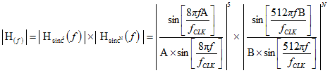
where
- f = signal frequency
- fCLK = ADC clock frequency
- A = First-stage decimation ratio (see Table 9-3)
- B = Second-stage decimation ratio (see Table 9-3)
- N = Second-stage filter order where N = 1 (sinc1), 2 (sinc2), 3 (sinc3), or 4 (sinc4)
The digital filter attenuates out-of-band noise that is present in the signal, and noise within the PGA and ADC modulator. Adjusting the filter by changing the decimation ratio and sinc order changes the filter bandwidth. Tradeoffs are made between signal bandwidth, noise, and filter latency.
As shown in Figure 9-14 and Figure 9-15, the first-stage sinc5 filter has frequency response nulls occurring at the data rate (fMOD / A) and at data rate multiples. At the null frequencies, the filter has zero gain.
") Figure 9-14 Sinc Frequency Response
Figure 9-14 Sinc Frequency Response (38400 SPS)
") Figure 9-15 Sinc Frequency Response
Figure 9-15 Sinc Frequency Response (14400 SPS)
The second stage superimposes new nulls in the frequency response over the nulls produced by the first stage. The first of the superimposed frequency response nulls occur at the output data rate, followed by nulls occurring at data rate multiples.
Figure 9-16 illustrates the frequency response of data rate 2400 SPS produced by the combined filter stages. This data rate has five equally-spaced nulls between the larger nulls produced by the first stage. The frequency response is also characteristic of data rates 2.5 SPS to 7200 SPS that are also produced by the second-stage filter. Figure 9-17 shows the frequency response nulls for 10 SPS.
") Figure 9-16 Sinc Frequency Response (2400 SPS)
Figure 9-16 Sinc Frequency Response (2400 SPS)") Figure 9-17 Sinc Frequency Response (10 SPS)
Figure 9-17 Sinc Frequency Response (10 SPS)Figure 9-18 and Figure 9-19 illustrate the frequency response of data rates 50 SPS and 60 SPS. The frequency response is plotted out to the 50-Hz 12th harmonic (10th harmonic for 60 Hz). The 50-Hz or 60-Hz fundamental frequency and harmonics are suppressed by increasing the second-stage filter order, as shown in the figures.
") Figure 9-18 Sinc Frequency Response (50 SPS)
Figure 9-18 Sinc Frequency Response (50 SPS)") Figure 9-19 Sinc Frequency Response (60 SPS)
Figure 9-19 Sinc Frequency Response (60 SPS)Figure 9-20 and Figure 9-21 plot the detailed frequency response of 50-SPS and 60-SPS data rates of different sinc-filter orders. Note that the high-order sinc filter increases the width of the null and improves line cycle rejection. The high-order filter decreases the sensitivity of the ratio tolerance between the ADC clock frequency and the line frequency that can otherwise degrade line cycle rejection. As shown in the plots, the best 50-Hz or 60-Hz rejection is provided by the sinc4 order, but has longer filter latency compared to the sinc1 order.
") Figure 9-20 Sinc Frequency Response Zoom
Figure 9-20 Sinc Frequency Response Zoom (50 SPS)
") Figure 9-21 Sinc Frequency Response Zoom
Figure 9-21 Sinc Frequency Response Zoom (60 SPS)
The overall sinc filter frequency has a low-pass response that rolls off high-frequency components in the signal. The signal bandwidth depends on the output data rate and the order of the sinc filter. Note the overall system bandwidth is the combination of the digital filter, the antialias filter, and external filter components. Table 9-4 lists the –3-dB filter bandwidth of the sinc filter. Note the bandwidth reduction of the higher-order sinc filters.
| DATA RATE (SPS) | -3-dB BANDWIDTH (Hz) | ||||
|---|---|---|---|---|---|
| SINC1 | SINC2 | SINC3 | SINC4 | SINC5 | |
| 2.5 | 1.10 | 0.80 | 0.65 | 0.58 | — |
| 5 | 2.23 | 1.60 | 1.33 | 1.15 | — |
| 10 | 4.43 | 3.20 | 2.62 | 2.28 | — |
| 16.6 | 7.38 | 5.33 | 4.37 | 3.80 | — |
| 20 | 8.85 | 6.38 | 5.25 | 4.63 | — |
| 50 | 22.1 | 16.0 | 13.1 | 11.4 | — |
| 60 | 26.6 | 19.1 | 15.7 | 13.7 | — |
| 100 | 44.3 | 31.9 | 26.2 | 22.8 | — |
| 400 | 177 | 128 | 105 | 91.0 | — |
| 1200 | 525 | 381 | 314 | 273 | — |
| 2400 | 1015 | 751 | 623 | 544 | — |
| 4800 | 1798 | 1421 | 1214 | 1077 | — |
| 7200 | 2310 | 1972 | 1750 | 1590 | — |
| 14400 | — | — | — | — | 2940 |
| 19200 | — | — | — | — | 3920 |
| 38400 | — | — | — | — | 7740 |