SBAS937B September 2018 – December 2018 ADS1278-SP
PRODUCTION DATA.
- 1 Features
- 2 Applications
- 3 Description
- 4 Revision History
- 5 Description (continued)
- 6 Pin Configuration and Functions
- 7 Specifications
-
8 Detailed Description
- 8.1 Overview
- 8.2 Functional Block Diagram
- 8.3
Feature Description
- 8.3.1 Sampling Aperture Matching
- 8.3.2 Frequency Response
- 8.3.3 Phase Response
- 8.3.4 Settling Time
- 8.3.5 Data Format
- 8.3.6 Analog Inputs (AINP, AINN)
- 8.3.7 Voltage Reference Inputs (VREFP, VREFN)
- 8.3.8 Clock Input (CLK)
- 8.3.9 Mode Selection (MODE)
- 8.3.10 Synchronization (SYNC)
- 8.3.11 Power-Down (PWDN)
- 8.3.12 Format[2:0]
- 8.3.13 Serial Interface Protocols
- 8.3.14 SPI Serial Interface
- 8.3.15 Frame-Sync Serial Interface
- 8.3.16 DOUT Modes
- 8.3.17 Daisy-Chaining
- 8.3.18 Modulator Output
- 8.3.19 Pin Test Using Test[1:0] Inputs
- 8.3.20 VCOM Output
- 8.4 Device Functional Modes
- 9 Application and Implementation
- 10Power Supply Recommendations
- 11Layout
- 12Device and Documentation Support
- 13Mechanical, Packaging, and Orderable Information
Package Options
Mechanical Data (Package|Pins)
- HFQ|84
Thermal pad, mechanical data (Package|Pins)
Orderable Information
10 Power Supply Recommendations
The ADS1278-SP has three power supplies: AVDD, DVDD, and IOVDD. AVDD is the analog supply that powers the modulator, DVDD is the digital supply that powers the digital core, and IOVDD is the digital I/O power supply. The IOVDD and DVDD power supplies can be tied together if desired (1.8 V). To achieve rated performance, it is critical that the power supplies are bypassed with 0.1-μF and 10-μF capacitors placed as close as possible to the supply pins. A single 10-μF ceramic capacitor may be substituted in place of the two capacitors.
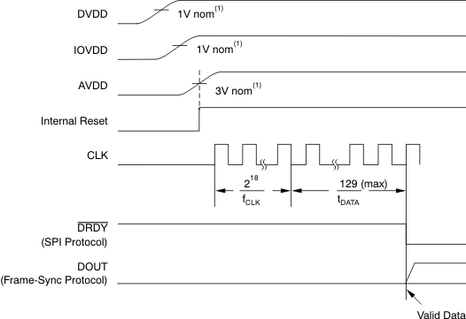
Figure 85 shows the start-up sequence of the ADS1278-SP. At power-on, bring up the DVDD supply first, followed by IOVDD and then AVDD. Check the power-supply sequence for proper order, including the ramp rate of each supply. DVDD and IOVDD may be sequenced at the same time if the supplies are tied together. Each supply has an internal reset circuit whose outputs are summed together to generate a global power-on reset. After the supplies have exceeded the reset thresholds, 218 fCLK cycles are counted before the converter initiates the conversion process. Following the CLK cycles, the data for 129 conversions are suppressed by the ADS1278-SP to allow output of fully-settled data. In SPI protocol, DRDY is held high during this interval. In frame-sync protocol, DOUT is forced to zero. The power supplies should be applied before any analog or digital pin is driven. For consistent performance, assert SYNC after device power-on when data first appear.
 Figure 85. Start-Up Sequence