SBAS590E March 2016 – June 2020 ADS131A02 , ADS131A04
PRODUCTION DATA.
- 1 Features
- 2 Applications
- 3 Description
- 4 Revision History
- 5 Device Comparison Table
- 6 Pin Configuration and Functions
-
7 Specifications
- 7.1 Absolute Maximum Ratings
- 7.2 ESD Ratings
- 7.3 Recommended Operating Conditions
- 7.4 Thermal Information
- 7.5 Electrical Characteristics
- 7.6 Timing Requirements: Asynchronous Interrupt Interface Mode
- 7.7 Switching Characteristics: Asynchronous Interrupt Interface Mode
- 7.8 Timing Requirements: Synchronous Master Interface Mode
- 7.9 Switching Characteristics: Synchronous Master Interface Mode
- 7.10 Timing Requirements: Synchronous Slave Interface Mode
- 7.11 Switching Characteristics: Synchronous Slave Interface Mode
- 7.12 Typical Characteristics
- 8 Parameter Measurement Information
-
9 Detailed Description
- 9.1 Overview
- 9.2 Functional Block Diagram
- 9.3 Feature Description
- 9.4 Device Functional Modes
- 9.5
Programming
- 9.5.1 Interface Protocol
- 9.5.2 SPI Interface
- 9.5.3
SPI Command Definitions
- 9.5.3.1 NULL: Null Command
- 9.5.3.2 RESET: Reset to POR Values
- 9.5.3.3 STANDBY: Enter Standby Mode
- 9.5.3.4 WAKEUP: Exit Standby Mode
- 9.5.3.5 LOCK: Lock ADC Registers
- 9.5.3.6 UNLOCK: Unlock ADC Registers
- 9.5.3.7 RREG: Read a Single Register
- 9.5.3.8 RREGS: Read Multiple Registers
- 9.5.3.9 WREG: Write Single Register
- 9.5.3.10 WREGS: Write Multiple Registers
- 9.6
Register Maps
- 9.6.1
User Register Description
- 9.6.1.1 ID_MSB: ID Control Register MSB (address = 00h) [reset = xxh]
- 9.6.1.2 ID_LSB: ID Control Register LSB (address = 01h) [reset = xxh]
- 9.6.1.3 STAT_1: Status 1 Register (address = 02h) [reset = 00h]
- 9.6.1.4 STAT_P: Positive Input Fault Detect Status Register (address = 03h) [reset = 00h]
- 9.6.1.5 STAT_N: Negative Input Fault Detect Status Register (address = 04h) [reset = 00h]
- 9.6.1.6 STAT_S: SPI Status Register (address = 05h) [reset = 00h]
- 9.6.1.7 ERROR_CNT: Error Count Register (address = 06h) [reset = 00h]
- 9.6.1.8 STAT_M2: Hardware Mode Pin Status Register (address = 07h) [reset = xxh]
- 9.6.1.9 Reserved Registers (address = 08h to 0Ah) [reset = 00h]
- 9.6.1.10 A_SYS_CFG: Analog System Configuration Register (address = 0Bh) [reset = 60h]
- 9.6.1.11 D_SYS_CFG: Digital System Configuration Register (address = 0Ch) [reset = 3Ch]
- 9.6.1.12 CLK1: Clock Configuration 1 Register (address = 0Dh) [reset = 08h]
- 9.6.1.13 CLK2: Clock Configuration 2 Register (address = 0Eh) [reset = 86h]
- 9.6.1.14 ADC_ENA: ADC Channel Enable Register (address = 0Fh) [reset = 00h]
- 9.6.1.15 Reserved Register (address = 10h) [reset = 00h]
- 9.6.2 ADCx: ADC Channel Digital Gain Configuration Registers (address = 11h to 14h) [reset = 00h]
- 9.6.1
User Register Description
- 10Application and Implementation
- 11Power Supply Recommendations
- 12Layout
- 13Device and Documentation Support
- 14Mechanical, Packaging, and Orderable Information
Package Options
Refer to the PDF data sheet for device specific package drawings
Mechanical Data (Package|Pins)
- PBS|32
Thermal pad, mechanical data (Package|Pins)
- PBS|32
Orderable Information
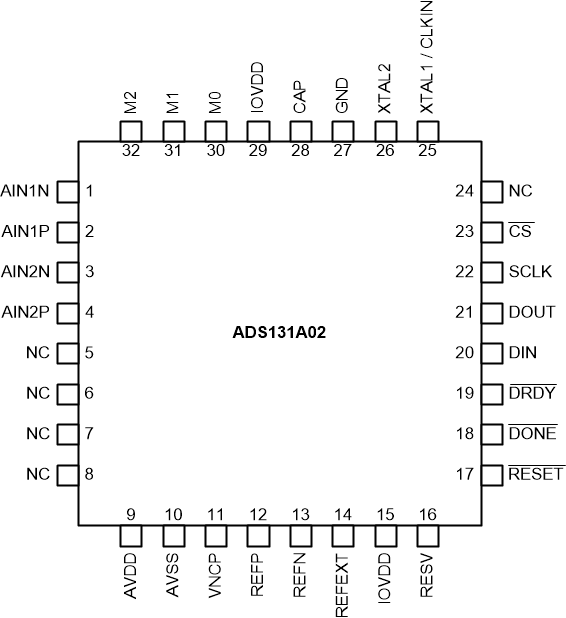
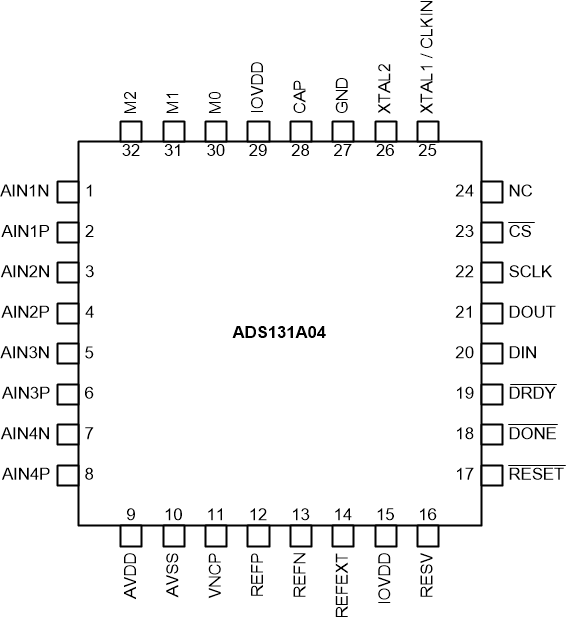
6 Pin Configuration and Functions
ADS131A02: PBS Package
32-Pin TQFP
Top View

ADS131A04: PBS Package
32-Pin TQFP
Top View

Pin Functions
| PIN | I/O | DESCRIPTION(2) | ||
|---|---|---|---|---|
| NAME | NO. | |||
| ADS131A02 | ADS131A04 | |||
| AIN1N | 1 | 1 | Analog input | Negative analog input 1 |
| AIN1P | 2 | 2 | Analog input | Positive analog input 1 |
| AIN2N | 3 | 3 | Analog input | Negative analog input 2 |
| AIN2P | 4 | 4 | Analog input | Positive analog input 2 |
| AIN3N | — | 5 | Analog input | Negative analog input 3 |
| AIN3P | — | 6 | Analog input | Positive analog input 3 |
| AIN4N | — | 7 | Analog input | Negative analog input 4 |
| AIN4P | — | 8 | Analog input | Positive analog input 4 |
| AVDD | 9 | 9 | Supply | Positive analog power supply. Connect a 1-µF capacitor to AVSS. |
| AVSS | 10 | 10 | Supply | Negative analog power supply |
| CAP | 28 | 28 | Analog output | Digital low-dropout (LDO) regulator output. Connect a 1-µF capacitor to GND. |
| CS | 23 | 23 | Digital input | Chip select; active low |
| DIN | 20 | 20 | Digital input | Serial data input |
| DONE | 18 | 18 | Digital output | Communication done signal; active low |
| DOUT | 21 | 21 | Digital output | Serial data output. Connect a 100-kΩ pullup resistor to IOVDD. |
| DRDY | 19 | 19 | Digital input/output | Data ready; active low; host interrupt and synchronization for multi-devices |
| GND | 27 | 27 | Supply | Digital ground |
| IOVDD | 15 | 15 | Supply | Digital I/O supply voltage. Connect a 1-µF capacitor to GND. |
| 29 | 29 | |||
| M0(1) | 30 | 30 | Digital input | Serial peripheral interface (SPI) configuration mode.
IOVDD: Asynchronous interrupt mode GND: Synchronous master mode No connection: Synchronous slave mode; use for multi-device mode |
| M1(1) | 31 | 31 | Digital input | SPI word transfer size.
IOVDD: 32 bit GND: 24 bit No connection: 16 bit |
| M2(1) | 32 | 32 | Digital input | Hamming code enable.
IOVDD: Hamming code word validation on GND: Hamming code word validation off No connection: reserved; do not use |
| NC | 5-8 | — | — | Leave floating or connect directly to AVSS. |
| NC | 24 | 24 | Digital output | Leave floating or tie to GND through a 10-kΩ pulldown resistor. |
| REFEXT | 14 | 14 | Analog input | Buffered external reference voltage input.
Connect a 1-µF capacitor to AVSS when using the internal reference. |
| REFN | 13 | 13 | Analog input | Negative reference voltage. Connect to AVSS. |
| REFP | 12 | 12 | Analog output | Positive reference voltage output. Connect a 1-µF capacitor to REFN. |
| RESET | 17 | 17 | Digital input | System reset; active low |
| RESV | 16 | 16 | Digital input | Reserved pin; connect to IOVDD |
| SCLK | 22 | 22 | Digital input/output | Serial data clock |
| VNCP | 11 | 11 | Analog output | Negative charge pump voltage output.
Connect a 270-nF capacitor to AVSS when enabling the negative charge pump. Connect directly to AVSS if the negative charge pump is unused. |
| XTAL1/CLKIN | 25 | 25 | Digital input | Master clock input, crystal oscillator buffer input |
| XTAL2 | 26 | 26 | Digital output | Crystal oscillator connection. Leave this pin floating if the crystal oscillator is unused. |
(1) Mode signal states are latched following a power-on-reset (POR). Tie these pins high or low with a resistance less than 1-kΩ resistor.
(2) See the Unused Inputs and Outputs section for unused pin connections.