SBASAA3 September 2021 ADS131B02-Q1
PRODUCTION DATA
- 1 Features
- 2 Applications
- 3 Description
- 4 Revision History
- 5 Pin Configuration and Functions
- 6 Specifications
- 7 Parameter Measurement Information
-
8 Detailed Description
- 8.1 Overview
- 8.2 Functional Block Diagram
- 8.3 Feature Description
- 8.4 Device Functional Modes
- 8.5
Programming
- 8.5.1
Serial Interface
- 8.5.1.1 Chip Select (CS)
- 8.5.1.2 Serial Data Clock (SCLK)
- 8.5.1.3 Serial Data Input (DIN)
- 8.5.1.4 Serial Data Output (DOUT)
- 8.5.1.5 Data Ready (DRDY)
- 8.5.1.6 SPI Communication Frames
- 8.5.1.7 SPI Communication Words
- 8.5.1.8 Short SPI Frames
- 8.5.1.9 Communication Cyclic Redundancy Check (CRC)
- 8.5.1.10 SPI Timeout
- 8.5.2 ADC Conversion Data Format
- 8.5.3 Commands
- 8.5.4 Collecting Data for the First Time or After a Pause in Data Collection
- 8.5.1
Serial Interface
- 8.6 Register Map
- 9 Application and Implementation
- 10Power Supply Recommendations
- 11Layout
- 12Device and Documentation Support
- 13Mechanical, Packaging, and Orderable Information
Package Options
Mechanical Data (Package|Pins)
- PW|20
Thermal pad, mechanical data (Package|Pins)
Orderable Information
8.3.8.2 Digital Filter Characteristic
Equation 4 calculates the z-domain transfer function of a sinc3 filter that is used for OSRs ranging from 128 to 1024:
Equation 4. 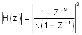
where:
- N is the OSR
Equation 5 calculates the transfer function of a sinc3 filter in terms of the continuous-time frequency parameter f:
Equation 5. 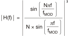
where:
- N is the OSR
Figure 8-5 and Figure 8-6 show the digital filter response of the fast-settling filter and the sinc3 filter for OSRs ranging from 128 to 1024. Figure 8-7 and Figure 8-8 compare the digital filter responses of the sinc3 filter at an OSR of 1024 and sinc3 + sinc1 filter for an OSR of 4096.
 Figure 8-5 Fast-Settling and Sinc3 Digital Filter Response
 Figure 8-7 Digital Filter Response for OSR = 1024 and OSR = 4096
 Figure 8-6 Fast-Settling and Sinc3 Digital Filter Response, Pass-Band
Detail
Figure 8-6 Fast-Settling and Sinc3 Digital Filter Response, Pass-Band
Detail Figure 8-8 Digital Filter Response for OSR = 1024 and OSR = 4096, Pass-Band
Detail
Figure 8-8 Digital Filter Response for OSR = 1024 and OSR = 4096, Pass-Band
Detail