SBAS853A January 2020 – April 2021 ADS131M02
PRODUCTION DATA
- 1 Features
- 2 Applications
- 3 Description
- 4 Revision History
- 5 Pin Configuration and Functions
- 6 Specifications
- 7 Parameter Measurement Information
-
8 Detailed Description
- 8.1 Overview
- 8.2 Functional Block Diagram
- 8.3
Feature Description
- 8.3.1 Input ESD Protection Circuitry
- 8.3.2 Input Multiplexer
- 8.3.3 Programmable Gain Amplifier (PGA)
- 8.3.4 Voltage Reference
- 8.3.5 Clocking and Power Modes
- 8.3.6 ΔΣ Modulator
- 8.3.7 Digital Filter
- 8.3.8 DC Block Filter
- 8.3.9 Internal Test Signals
- 8.3.10 Channel Phase Calibration
- 8.3.11 Calibration Registers
- 8.3.12 Communication Cyclic Redundancy Check (CRC)
- 8.3.13 Register Map CRC
- 8.4 Device Functional Modes
- 8.5
Programming
- 8.5.1
Interface
- 8.5.1.1 Chip Select (CS)
- 8.5.1.2 Serial Data Clock (SCLK)
- 8.5.1.3 Serial Data Input (DIN)
- 8.5.1.4 Serial Data Output (DOUT)
- 8.5.1.5 Data Ready (DRDY)
- 8.5.1.6 Conversion Synchronization or System Reset (SYNC/RESET)
- 8.5.1.7 SPI Communication Frames
- 8.5.1.8 SPI Communication Words
- 8.5.1.9 ADC Conversion Data
- 8.5.1.10
Commands
- 8.5.1.10.1 NULL (0000 0000 0000 0000)
- 8.5.1.10.2 RESET (0000 0000 0001 0001)
- 8.5.1.10.3 STANDBY (0000 0000 0010 0010)
- 8.5.1.10.4 WAKEUP (0000 0000 0011 0011)
- 8.5.1.10.5 LOCK (0000 0101 0101 0101)
- 8.5.1.10.6 UNLOCK (0000 0110 0110 0110)
- 8.5.1.10.7 RREG (101a aaaa annn nnnn)
- 8.5.1.10.8 WREG (011a aaaa annn nnnn)
- 8.5.1.11 Short SPI Frames
- 8.5.2 Synchronization
- 8.5.1
Interface
- 8.6 ADS131M02 Registers
- 9 Application and Implementation
- 10Power Supply Recommendations
- 11Layout
- 12Device and Documentation Support
- 13Mechanical, Packaging, and Orderable Information
Package Options
Mechanical Data (Package|Pins)
Thermal pad, mechanical data (Package|Pins)
- RUK|20
Orderable Information
9.2.2.4 Calibration
Certain signal chain errors can be corrected through a single room temperature calibration. The ADS131M02 has the capability to store calibration values and use the values to correct the results in real time. Among those errors that can be corrected in real time with the ADS131M02 are offset error, gain error, and phase error.
Offset calibration is performed by determining the measured output of the signal chain when the input is zero voltage for a voltage channel or zero current for a current channel. The value can be measured and recorded in external non-volatile memory for each channel. When the system is deployed, these values can be provided to the CHn_OCAL_MSB and CHn_OCAL_LSB registers for the corresponding channels. The ADS131M02 then subtracts these values from its conversion results prior to providing them to the host. Alternatively, the integrated DC block filter can be used to implement offset correction.
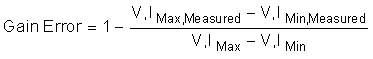
Similar to offset error correction, system gain error can be determined prior to deployment and can be used to correct the gain error on each channel in real time. Gain error is defined as the percentage difference in the ADC transfer function from its PGA gain corrected ideal value of 1. This error can be determined by measuring the results from both a maximum and minimum input signal, finding the difference between these results, and dividing by the difference between the ideal difference. Equation 13 describes how to calculate gain error.
To correct for gain error, divide each offset-corrected conversion result by the measured gain. The ADS131M02 multiplies each conversion result by the calibration factor stored in the CHn_GCAL_MSB and CHn_GCAL_LSB registers according to the method described in the Section 8.3.11 section. The host can program the measured inverted gain values for each channel into these registers to have them automatically corrected for each sample.
The ADS131M02 can also correct for system phase error introduced by sensors. For this design, the CT introduces some phase error into the system. This design uses a software method for phase correction, but the ADS131M02 can perform this function in real time. The system must first measure the phase relationships between the various channels. Then, define one channel as phase 0. Subsequently, the PHASEn bits in the CHn_CFG registers corresponding to the various other channels can be edited to correct their phase relationship relative to the phase 0 channels.