SBAS889A January 2020 – April 2021 ADS131M03
PRODUCTION DATA
- 1 Features
- 2 Applications
- 3 Description
- 4 Revision History
- 5 Pin Configuration and Functions
- 6 Specifications
- 7 Parameter Measurement Information
-
8 Detailed Description
- 8.1 Overview
- 8.2 Functional Block Diagram
- 8.3
Feature Description
- 8.3.1 Input ESD Protection Circuitry
- 8.3.2 Input Multiplexer
- 8.3.3 Programmable Gain Amplifier (PGA)
- 8.3.4 Voltage Reference
- 8.3.5 Clocking and Power Modes
- 8.3.6 ΔΣ Modulator
- 8.3.7 Digital Filter
- 8.3.8 DC Block Filter
- 8.3.9 Internal Test Signals
- 8.3.10 Channel Phase Calibration
- 8.3.11 Calibration Registers
- 8.3.12 Communication Cyclic Redundancy Check (CRC)
- 8.3.13 Register Map CRC
- 8.4 Device Functional Modes
- 8.5
Programming
- 8.5.1
Interface
- 8.5.1.1 Chip Select (CS)
- 8.5.1.2 Serial Data Clock (SCLK)
- 8.5.1.3 Serial Data Input (DIN)
- 8.5.1.4 Serial Data Output (DOUT)
- 8.5.1.5 Data Ready (DRDY)
- 8.5.1.6 Conversion Synchronization or System Reset (SYNC/RESET)
- 8.5.1.7 SPI Communication Frames
- 8.5.1.8 SPI Communication Words
- 8.5.1.9 ADC Conversion Data
- 8.5.1.10
Commands
- 8.5.1.10.1 NULL (0000 0000 0000 0000)
- 8.5.1.10.2 RESET (0000 0000 0001 0001)
- 8.5.1.10.3 STANDBY (0000 0000 0010 0010)
- 8.5.1.10.4 WAKEUP (0000 0000 0011 0011)
- 8.5.1.10.5 LOCK (0000 0101 0101 0101)
- 8.5.1.10.6 UNLOCK (0000 0110 0110 0110)
- 8.5.1.10.7 RREG (101a aaaa annn nnnn)
- 8.5.1.10.8 WREG (011a aaaa annn nnnn)
- 8.5.1.11 Short SPI Frames
- 8.5.2 Synchronization
- 8.5.1
Interface
- 8.6 ADS131M03 Registers
- 9 Application and Implementation
- 10Power Supply Recommendations
- 11Layout
- 12Device and Documentation Support
- 13Mechanical, Packaging, and Orderable Information
Package Options
Mechanical Data (Package|Pins)
Thermal pad, mechanical data (Package|Pins)
Orderable Information
9.2.2.2 Current Measurement Front-End
The analog front-end for current inputs is different from the analog front-end for the voltage inputs. Figure 9-7 shows the analog front-end used for a current channel.
 Figure 9-7 Current Measurement Front-End
The analog front-end for current consists of burden resistors for the current transformers (RB) and an RC low-pass filter (RFILT and CFILT) that functions as an antialias filter.
Two identical burden resistors in series are used with the common point being connected to GND instead of using one burden resistor for best THD performance. This split-burden resistor configuration ensures that the waveforms fed to the positive and negative terminals of the ADC are 180 degrees out-of-phase with each other, which provides the best THD results with this ADC. The total burden resistance is selected based on the current range used and the turns ratio specification of the CT (this design uses CTs with a turns ratio of 2000). The total value of the effective burden resistor (2RB) for this design is 12.98 Ω.
Equation 12 shows how to calculate the range of differential voltages fed to the current ADC channel for a given maximum current, CT turns ratio, and burden resistor value.
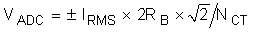
Based on the maximum RMS current of 100 A, a CT turns ratio NCT of 2000, and an effective burden resistor 2RB between AINxP and AINxN of 12.98 Ω for this design, the input signal to the current ADC has a voltage swing of ±918 mV maximum (649 mVRMS) when the maximum current rating of the meter (100 A) is applied. This ±918-mV maximum input voltage is well within the ±1.2-V input range of the device for the selected PGA gain of 1 that is used for the current channels.