SBASAF2 August 2022 ADS131M06-Q1
PRODUCTION DATA
- 1 Features
- 2 Applications
- 3 Description
- 4 Revision History
- 5 Pin Configuration and Functions
- 6 Specifications
- 7 Parameter Measurement Information
-
8 Detailed Description
- 8.1 Overview
- 8.2 Functional Block Diagram
- 8.3
Feature Description
- 8.3.1 Input ESD Protection Circuitry
- 8.3.2 Input Multiplexer
- 8.3.3 Programmable Gain Amplifier (PGA)
- 8.3.4 Voltage Reference
- 8.3.5 Clocking and Power Modes
- 8.3.6 ΔΣ Modulator
- 8.3.7 Digital Filter
- 8.3.8 DC Block Filter
- 8.3.9 Internal Test Signals
- 8.3.10 Channel Phase Calibration
- 8.3.11 Calibration Registers
- 8.3.12 Communication Cyclic Redundancy Check (CRC)
- 8.3.13 Register Map CRC
- 8.4 Device Functional Modes
- 8.5
Programming
- 8.5.1
Interface
- 8.5.1.1 Chip Select (CS)
- 8.5.1.2 Serial Data Clock (SCLK)
- 8.5.1.3 Serial Data Input (DIN)
- 8.5.1.4 Serial Data Output (DOUT)
- 8.5.1.5 Data Ready (DRDY)
- 8.5.1.6 Conversion Synchronization or System Reset (SYNC/RESET)
- 8.5.1.7 SPI Communication Frames
- 8.5.1.8 SPI Communication Words
- 8.5.1.9 ADC Conversion Data
- 8.5.1.10
Commands
- 8.5.1.10.1 NULL (0000 0000 0000 0000)
- 8.5.1.10.2 RESET (0000 0000 0001 0001)
- 8.5.1.10.3 STANDBY (0000 0000 0010 0010)
- 8.5.1.10.4 WAKEUP (0000 0000 0011 0011)
- 8.5.1.10.5 LOCK (0000 0101 0101 0101)
- 8.5.1.10.6 UNLOCK (0000 0110 0101 0101)
- 8.5.1.10.7 RREG (101a aaaa annn nnnn)
- 8.5.1.10.8 WREG (011a aaaa annn nnnn)
- 8.5.1.11 Short SPI Frames
- 8.5.2 Synchronization
- 8.5.1
Interface
- 8.6 Registers
- 9 Application and Implementation
- 10Device and Documentation Support
- 11Mechanical, Packaging, and Orderable Information
Package Options
Mechanical Data (Package|Pins)
- PBS|32
Thermal pad, mechanical data (Package|Pins)
- PBS|32
Orderable Information
7.1 Noise Measurements
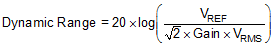
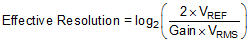
Adjust the data rate and gain to optimize the ADS131M06-Q1 noise performance. When averaging is increased by reducing the data rate, noise drops correspondingly. Table 7-1 summarizes the ADS131M06-Q1 noise performance using the 1.2-V internal reference and a 3.0-V analog power supply. The data are representative of typical noise performance at TA = 25°C when fCLKIN = 8.192 MHz. The modulator clock frequency fMOD is equal to fCLKIN / 2. The data shown are typical input-referred noise results with the analog inputs shorted together and taking an average of multiple readings across all channels. A minimum 1 second of consecutive readings are used to calculate the RMS. Table 7-2 shows the dynamic range and effective resolution calculated from the noise data. Equation 1 calculates dynamic range. Equation 2 calculates effective resolution. In each case, VREF corresponds to the internal 1.2-V reference, or the voltage on the REFIN pin if the external reference is used. In global-chop mode, noise is improved by a factor of √ 2.
The noise performance scales with the OSR and gain settings, but is independent from the configured power mode. Thus, the device exhibits the same noise performance in different power modes when selecting the same OSR and gain settings. However, the data rate at the OSR settings scales based on the applied clock frequency for the different power modes.
| OSR | DATA RATE (kSPS), fCLKIN = 8.192 MHz |
GAIN | |||||||
|---|---|---|---|---|---|---|---|---|---|
| 1 | 2 | 4 | 8 | 16 | 32 | 64 | 128 | ||
| 16384 | 0.25 | 1.90 | 1.69 | 1.56 | 0.95 | 0.64 | 0.42 | 0.42 | 0.42 |
| 8192 | 0.5 | 2.39 | 2.13 | 2.13 | 1.29 | 0.86 | 0.57 | 0.57 | 0.57 |
| 4096 | 1 | 3.38 | 2.99 | 2.88 | 1.74 | 1.17 | 0.77 | 0.77 | 0.77 |
| 2048 | 2 | 4.25 | 3.91 | 3.79 | 2.27 | 1.52 | 1.00 | 1.00 | 1.00 |
| 1024 | 4 | 5.35 | 4.68 | 4.52 | 2.70 | 1.82 | 1.20 | 1.20 | 1.20 |
| 512 | 8 | 7.56 | 6.62 | 6.37 | 3.82 | 2.55 | 1.69 | 1.69 | 1.69 |
| 256 | 16 | 10.68 | 9.56 | 9.09 | 5.42 | 3.63 | 2.39 | 2.39 | 2.40 |
| 128 | 32 | 21.31 | 15.26 | 13.52 | 7.89 | 5.21 | 3.41 | 3.42 | 3.42 |
| OSR | DATA RATE (kSPS), fCLKIN = 8.192 MHz |
GAIN | |||||||
|---|---|---|---|---|---|---|---|---|---|
| 1 | 2 | 4 | 8 | 16 | 32 | 64 | 128 | ||
| 16384 | 0.25 | 113 (20.3) | 108 (19.4) | 103 (18.6) | 101 (18.3) | 98 (17.8) | 96 (17.5) | 90 (16.5) | 84 (15.4) |
| 8192 | 0.5 | 111 (19.9) | 106 (19.1) | 100 (18.1) | 98 (17.8) | 96 (17.4) | 93 (17.0) | 87 (16.0) | 81 (15.0) |
| 4096 | 1 | 108 (19.4) | 103 (18.6) | 97 (17.7) | 96 (17.4) | 93 (17.0) | 91 (16.6) | 85 (15.6) | 79 (14.6) |
| 2048 | 2 | 106 (19.1) | 101 (18.2) | 95 (17.3) | 93 (17.0) | 91 (16.6) | 88 (16.2) | 82 (15.2) | 76 (14.2) |
| 1024 | 4 | 104 (18.8) | 99 (18.0) | 93 (17.0) | 92 (16.8) | 89 (16.3) | 87 (15.9) | 81 (14.9) | 75 (13.9) |
| 512 | 8 | 101 (18.3) | 96 (17.5) | 90 (16.5) | 89 (16.3) | 86 (15.8) | 84 (15.4) | 78 (14.4) | 72 (13.4) |
| 256 | 16 | 98 (17.8) | 93 (16.9) | 87 (16.0) | 86 (15.8) | 83 (15.3) | 81 (14.9) | 75 (13.9) | 69 (12.9) |
| 128 | 32 | 92 (16.8) | 89 (16.3) | 84 (15.4) | 83 (15.2) | 80 (14.8) | 78 (14.4) | 72 (13.4) | 65 (12.4) |