SBASAF2 August 2022 ADS131M06-Q1
PRODUCTION DATA
- 1 Features
- 2 Applications
- 3 Description
- 4 Revision History
- 5 Pin Configuration and Functions
- 6 Specifications
- 7 Parameter Measurement Information
-
8 Detailed Description
- 8.1 Overview
- 8.2 Functional Block Diagram
- 8.3
Feature Description
- 8.3.1 Input ESD Protection Circuitry
- 8.3.2 Input Multiplexer
- 8.3.3 Programmable Gain Amplifier (PGA)
- 8.3.4 Voltage Reference
- 8.3.5 Clocking and Power Modes
- 8.3.6 ΔΣ Modulator
- 8.3.7 Digital Filter
- 8.3.8 DC Block Filter
- 8.3.9 Internal Test Signals
- 8.3.10 Channel Phase Calibration
- 8.3.11 Calibration Registers
- 8.3.12 Communication Cyclic Redundancy Check (CRC)
- 8.3.13 Register Map CRC
- 8.4 Device Functional Modes
- 8.5
Programming
- 8.5.1
Interface
- 8.5.1.1 Chip Select (CS)
- 8.5.1.2 Serial Data Clock (SCLK)
- 8.5.1.3 Serial Data Input (DIN)
- 8.5.1.4 Serial Data Output (DOUT)
- 8.5.1.5 Data Ready (DRDY)
- 8.5.1.6 Conversion Synchronization or System Reset (SYNC/RESET)
- 8.5.1.7 SPI Communication Frames
- 8.5.1.8 SPI Communication Words
- 8.5.1.9 ADC Conversion Data
- 8.5.1.10
Commands
- 8.5.1.10.1 NULL (0000 0000 0000 0000)
- 8.5.1.10.2 RESET (0000 0000 0001 0001)
- 8.5.1.10.3 STANDBY (0000 0000 0010 0010)
- 8.5.1.10.4 WAKEUP (0000 0000 0011 0011)
- 8.5.1.10.5 LOCK (0000 0101 0101 0101)
- 8.5.1.10.6 UNLOCK (0000 0110 0101 0101)
- 8.5.1.10.7 RREG (101a aaaa annn nnnn)
- 8.5.1.10.8 WREG (011a aaaa annn nnnn)
- 8.5.1.11 Short SPI Frames
- 8.5.2 Synchronization
- 8.5.1
Interface
- 8.6 Registers
- 9 Application and Implementation
- 10Device and Documentation Support
- 11Mechanical, Packaging, and Orderable Information
Package Options
Mechanical Data (Package|Pins)
- PBS|32
Thermal pad, mechanical data (Package|Pins)
- PBS|32
Orderable Information
8.3.7.2 Digital Filter Characteristic
Equation 6 calculates the z-domain transfer function of a sinc3 filter that is used for OSRs of 1024 and lower.
Equation 6. 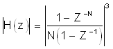
where N is the OSR.
Equation 7 calculates the transfer function of a sinc3 filter in terms of the continuous-time frequency parameter f.
Equation 7. 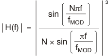
where N is the OSR.
Figure 8-4 and Figure 8-5 show the digital filter response of the fast-settling filter and the sinc3 filter for OSRs of 1024 and lower. Figure 8-6 and Figure 8-7 show the digital filter response of the sinc3 + sinc1 filter for an OSR of 4096.
 Figure 8-4 Fast-Settling and
Sinc3 Digital Filter Response
Figure 8-4 Fast-Settling and
Sinc3 Digital Filter Response Figure 8-6 Digital Filter Response for OSR
= 1024 and OSR = 4096
Figure 8-6 Digital Filter Response for OSR
= 1024 and OSR = 4096 Figure 8-5 Fast-Settling and
Sinc3 Digital Filter Response,
Pass-Band Detail
Figure 8-5 Fast-Settling and
Sinc3 Digital Filter Response,
Pass-Band Detail Figure 8-7 Digital Filter Response for OSR
= 1024 and OSR = 4096, Pass-Band Detail
Figure 8-7 Digital Filter Response for OSR
= 1024 and OSR = 4096, Pass-Band Detail