SBAS950B October 2019 – February 2021 ADS131M08
PRODUCTION DATA
- 1 Features
- 2 Applications
- 3 Description
- 4 Revision History
- 5 Pin Configuration and Functions
- 6 Specifications
- 7 Parameter Measurement Information
-
8 Detailed Description
- 8.1 Overview
- 8.2 Functional Block Diagram
- 8.3
Feature Description
- 8.3.1 Input ESD Protection Circuitry
- 8.3.2 Input Multiplexer
- 8.3.3 Programmable Gain Amplifier (PGA)
- 8.3.4 Voltage Reference
- 8.3.5 Clocking and Power Modes
- 8.3.6 ΔΣ Modulator
- 8.3.7 Digital Filter
- 8.3.8 DC Block Filter
- 8.3.9 Internal Test Signals
- 8.3.10 Channel Phase Calibration
- 8.3.11 Calibration Registers
- 8.3.12 Communication Cyclic Redundancy Check (CRC)
- 8.3.13 Register Map CRC
- 8.4 Device Functional Modes
- 8.5
Programming
- 8.5.1
Interface
- 8.5.1.1 Chip Select (CS)
- 8.5.1.2 Serial Data Clock (SCLK)
- 8.5.1.3 Serial Data Input (DIN)
- 8.5.1.4 Serial Data Output (DOUT)
- 8.5.1.5 Data Ready (DRDY)
- 8.5.1.6 Conversion Synchronization or System Reset (SYNC/RESET)
- 8.5.1.7 SPI Communication Frames
- 8.5.1.8 SPI Communication Words
- 8.5.1.9 ADC Conversion Data
- 8.5.1.10
Commands
- 8.5.1.10.1 NULL (0000 0000 0000 0000)
- 8.5.1.10.2 RESET (0000 0000 0001 0001)
- 8.5.1.10.3 STANDBY (0000 0000 0010 0010)
- 8.5.1.10.4 WAKEUP (0000 0000 0011 0011)
- 8.5.1.10.5 LOCK (0000 0101 0101 0101)
- 8.5.1.10.6 UNLOCK (0000 0110 0110 0110)
- 8.5.1.10.7 RREG (101a aaaa annn nnnn)
- 8.5.1.10.8 WREG (011a aaaa annn nnnn)
- 8.5.1.11 Short SPI Frames
- 8.5.2 Synchronization
- 8.5.1
Interface
- 8.6 Registers
- 9 Application and Implementation
- 10Power Supply Recommendations
- 11Layout
- 12Device and Documentation Support
- 13Mechanical, Packaging, and Orderable Information
Package Options
Mechanical Data (Package|Pins)
Thermal pad, mechanical data (Package|Pins)
Orderable Information
9.2.2.1 Voltage Measurement Front-End
The nominal voltage from the mains is from 100 V – 240 V so this voltage must be scaled down to be sensed by an ADC. Figure 9-6 shows the analog front-end used for this voltage scaling.
 Figure 9-6 Voltage Measurement Front-End
The analog front-end for voltage consists of a spike protection varistor (RV), a voltage divider network (RHI and RLO), and an RC low-pass filter (RFILT and CFILT).
Equation 11 shows how to calculate the range of differential voltages fed to the voltage ADC channel for a given mains voltage and the selected voltage divider resistor values.
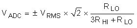
RHI is 300 kΩ and RLO is 750 Ω in this design. For a mains voltage of 240 V (as measured between the line and neutral), the input signal to the voltage ADC has a voltage swing of ±256 mV (182 mVRMS) based on Equation 11 and the selected resistor values. This voltage is well within the ±1.2-V input voltage range that can be sensed by the ADS131M08 for the selected PGA gain value of 1 that is used for the voltage channels.