SBAS603B April 2013 – November 2020 ADS4449
PRODUCTION DATA
- 1 Features
- 2 Applications
- 3 Description
- 4 Revision History
- 5 Pin Configuration and Functions
- 6 Specifications
- 7 Parameter Measurement Information
-
8 Detailed Description
- 8.1 Overview
- 8.2 Functional Block Diagram
- 8.3 Feature Description
- 8.4 Device Functional Modes
- 8.5 Programming
- 8.6
Register Maps
- 8.6.1
Register Description
- 8.6.1.1 Register Address 00h (Default = 00h)
- 8.6.1.2 Register Address 01h (Default = 00h)
- 8.6.1.3 Register Address 25h (Default = 00h)
- 8.6.1.4 Register Address 2bh (Default = 00h)
- 8.6.1.5 Register Address 31h (Default = 00h)
- 8.6.1.6 Register Address 37h (Default = 00h)
- 8.6.1.7 Register Address 3dh (Default = 00h)
- 8.6.1.8 Register Address 3fh (Default = 00h)
- 8.6.1.9 Register Address 40h (Default = 00h)
- 8.6.1.10 Register Address 42h (Default = 00h)
- 8.6.1.11 Register Address 45h (Default = 00h)
- 8.6.1.12 Register Address 4ah (Defalut = 00h)
- 8.6.1.13 Register Address 62h (Default = 00h)
- 8.6.1.14 Register Address 7ah (Default = 00h)
- 8.6.1.15 Register Address 92h (Default = 00h)
- 8.6.1.16 Register Address A9h (Default = 00h)
- 8.6.1.17 Register Address Ach (Default = 00h)
- 8.6.1.18 Register Address C3h (Default = 00h)
- 8.6.1.19 Register Address C4h (Default = 00h)
- 8.6.1.20 Register Address Cfh (Default = 00h)
- 8.6.1.21 Register Address D6h (Default = 00h)
- 8.6.1.22 Register Address D7h (Default = 00h)
- 8.6.1.23 Register Address F1h (Default = 00h)
- 8.6.1.24 Register Address 58h (Default = 00h)
- 8.6.1.25 Register Address 59h (Default = 00h)
- 8.6.1.26 Register Address 70h (Default = 00h)
- 8.6.1.27 Register Address 71h (Default = 00h)
- 8.6.1.28 Register Address 88h (Default = 00h)
- 8.6.1.29 Register Address 89h (Default = 00h)
- 8.6.1.30 Register Address A0h (Default = 00h)
- 8.6.1.31 Register Address A1h (Default = 00h)
- 8.6.1.32 Register Address Feh (Default = 00h)
- 8.6.1
Register Description
- 9 Application and Implementation
- 10Power Supply Recommendations
- 11Layout
- 12Device and Documentation Support
Package Options
Mechanical Data (Package|Pins)
- ZCR|144
Thermal pad, mechanical data (Package|Pins)
Orderable Information
8.5.1.2 Serial Register Readout
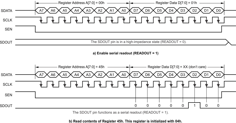
The device includes a mode where the contents of the internal registers can be read back, as shown in Figure 8-9. This readback mode can be useful as a diagnostic check to verify the serial interface communication between the external controller and ADC.
- Set the READOUT register bit to 1. This setting disables any further writes to the registers except register address 00h.
- Initiate a serial interface cycle specifying the address of the register (A[7:0]) whose content must be read.
- The device outputs the contents (D[7:0]) of the selected register on the SDOUT terminal (terminal G10).
- The external controller can latch the contents at the SCLK falling edge.
- To enable register writes, reset the READOUT register bit to 0.
Note that the contents of register 00h cannot be read back because the register contains RESET and READOUT bits. When the READOUT bit is disabled, the SDOUT terminal is in a high-impedance state. If serial readout is not used, the SDOUT terminal must not be connected (must float).
 Figure 8-9 Serial Readout Timing Diagram
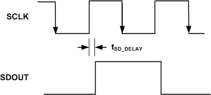
SDOUT comes out at the SCLK rising edge with an approximate delay (tSD_DELAY) of 8 ns, as shown in Figure 8-10.
 Figure 8-10 Sdout Delay Timing