SBAS928C February   2020  – September 2023 ADS7066

PRODUCTION DATA  

  1.   1
  2. Features
  3. Applications
  4. Description
  5. Revision History
  6. Pin Configuration and Functions
  7. Specifications
    1. 6.1 Absolute Maximum Ratings
    2. 6.2 ESD Ratings
    3. 6.3 Recommended Operating Conditions
    4. 6.4 Thermal Information
    5. 6.5 Electrical Characteristics
    6. 6.6 Timing Requirements
    7. 6.7 Switching Characteristics
    8. 6.8 Timing Diagrams
    9. 6.9 Typical Characteristics
  8. Detailed Description
    1. 7.1 Overview
    2. 7.2 Functional Block Diagram
    3. 7.3 Feature Description
      1. 7.3.1  Analog Input and Multiplexer
      2. 7.3.2  Reference
        1. 7.3.2.1 External Reference
        2. 7.3.2.2 Internal Reference
      3. 7.3.3  ADC Transfer Function
      4. 7.3.4  ADC Offset Calibration
      5. 7.3.5  Programmable Averaging Filters
      6. 7.3.6  CRC on Data Interface
      7. 7.3.7  Oscillator and Timing Control
      8. 7.3.8  Diagnostic Modes
        1. 7.3.8.1 Bit-Walk Test Mode
        2. 7.3.8.2 Fixed Voltage Test Mode
      9. 7.3.9  Output Data Format
        1. 7.3.9.1 Status Flags
        2. 7.3.9.2 Output CRC (Device to Host)
        3. 7.3.9.3 Input CRC (Host to Device)
      10. 7.3.10 Device Programming
        1. 7.3.10.1 Enhanced-SPI Interface
        2. 7.3.10.2 Daisy-Chain Mode
        3. 7.3.10.3 Register Read/Write Operation
          1. 7.3.10.3.1 Register Write
          2. 7.3.10.3.2 Register Read
            1. 7.3.10.3.2.1 Register Read With CRC
    4. 7.4 Device Functional Modes
      1. 7.4.1 Device Power-Up and Reset
      2. 7.4.2 Manual Mode
      3. 7.4.3 On-the-Fly Mode
      4. 7.4.4 Auto-Sequence Mode
    5. 7.5 ADS7066 Registers
  9. Application and Implementation
    1. 8.1 Application Information
    2. 8.2 Typical Application
      1. 8.2.1 Design Requirements
      2. 8.2.2 Detailed Design Procedure
        1. 8.2.2.1 Charge-Kickback Filter and ADC Amplifier
      3. 8.2.3 Application Curve
    3. 8.3 Power Supply Recommendations
      1. 8.3.1 AVDD and DVDD Supply Recommendations
    4. 8.4 Layout
      1. 8.4.1 Layout Guidelines
      2. 8.4.2 Layout Example
  10. Device and Documentation Support
    1. 9.1 Device Support
      1. 9.1.1 Development Support
    2. 9.2 Documentation Support
      1. 9.2.1 Related Documentation
    3. 9.3 Receiving Notification of Documentation Updates
    4. 9.4 Support Resources
    5. 9.5 Trademarks
    6. 9.6 Electrostatic Discharge Caution
    7. 9.7 Glossary
  11. 10Mechanical, Packaging, and Orderable Information

Package Options

Mechanical Data (Package|Pins)
Thermal pad, mechanical data (Package|Pins)
Orderable Information

Charge-Kickback Filter and ADC Amplifier

As illustrated in Figure 8-1, a filter capacitor (CFLT) is connected from each input pin of the ADC to ground. This capacitor helps reduce the sampling charge injection and provides a charge bucket to quickly charge the internal sample-and-hold capacitors during the acquisition process. This capacitor must be a COG- or NPO-type. One method for determining the required amplifier bandwidth and the values of the RC charge-kickback filter is provided in this section. This optimization and more details on the math behind the component selection are covered in ADC Precision Labs.

The minimum bandwidth of the amplifier for driving the ADC can be computed using the settling accuracy (0.5 LSB) and settling time (acquisition time) information. Equation 4, Equation 5, Equation 6, and Equation 7 compute the unity-gain bandwidth (UGBW) of the amplifier.

Equation 4. GUID-F9323050-EFFF-46E2-B144-5B3B86129317-low.gif
Equation 5. GUID-4F8CDD10-0565-4E0B-A413-16EF1FE405A0-low.gif
Equation 6. GUID-ABF615ED-2B46-4988-B3D4-A4081B084ECF-low.gif
Equation 7. GUID-52C0E426-34E1-4AA7-A6FE-C9AB903E2D22-low.gif

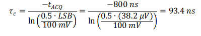
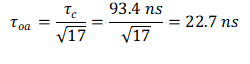
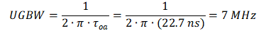
Based on the result of Equation 7, select an amplifier that has more than 7-MHz UGBW. For this example, OPA325 is used.

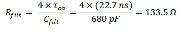
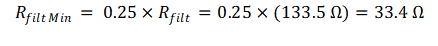
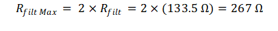
The value of Cfilt is computed in Equation 8 by taking 20 times the internal sample-and-hold capacitance. The factor of 20 is a rule of thumb that is intended to minimize the droop in voltage on the charge-bucket capacitor, Cfilt, after the start of the acquisition period. The filter resistor, Rfilt, is computed in Equation 9 using the op-amp time constant and Cfilt. Equation 10 and Equation 11 compute the minimum and maximum Rfilt values, respectively.

Equation 8. GUID-06CA1AD6-DD0A-47D3-817F-9291DE733042-low.gif

The value of Cfllt can be approximated to the nearest standard value 680 pF.

Equation 9. GUID-37F72A75-8507-4F54-9691-F1A9D45F1E13-low.gif
Equation 10. GUID-75F64B72-95E2-4B4B-B7A7-610D557873E7-low.gif
Equation 11. GUID-2D82B365-9807-4577-93A5-6965A79908F4-low.gif