SLAS492B September 2005 – August 2016 ADS7886
PRODUCTION DATA.
- 1 Features
- 2 Applications
- 3 Description
- 4 Revision History
- 5 Device Comparison Table
- 6 Pin Configuration and Functions
- 7 Specifications
- 8 Detailed Description
- 9 Application and Implementation
- 10Power Supply Recommendations
- 11Layout
- 12Device and Documentation Support
- 13Mechanical, Packaging, and Orderable Information
Package Options
Mechanical Data (Package|Pins)
Thermal pad, mechanical data (Package|Pins)
Orderable Information
1 Features
- 1-MHz Sample Rate Serial Device
- 12-Bit Resolution
- Zero Latency
- 20-MHz Serial Interface
- Supply Range: 2.35 V to 5.25 V
- Typical Power Dissipation at 1 MSPS:
- 3.9 mW at 3-V VDD
- 7.5 mW at 5-V VDD
- INL ±1.25 LSB Maximum, ±0.65 LSB (Typical)
- DNL ±1 LSB Maximum, +0.4 / –0.65 LSB (Typical)
- Typical AC Performance:
72.25-dB SINAD, –84-dB THD - Unipolar Input Range: 0 V to VDD
- Power Down Current: 1 µA
- Wide Input Bandwidth: 15 MHz at 3 dB
- 6-Pin SOT-23 and SC70 Packages
2 Applications
- Base Band Converters in Radio
Communication - Motor Current and Bus Voltage Sensors in Digital Drives
- Optical Networking (DWDM, MEMS Based Switching)
- Optical Sensors
- Battery-Powered Systems
- Medical Instrumentations
- High-Speed Data Acquisition Systems
- High-Speed Closed-Loop Systems
3 Description
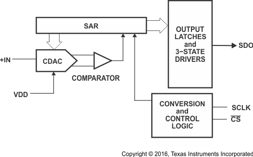
The ADS7886 is a 12-bit, 1-MSPS analog-to-digital converter (ADC). The device includes a capacitor based SAR A/D converter with inherent sample and hold. The serial interface in each device is controlled by the CS and SCLK signals for glueless connections with microprocessors and DSPs. The input signal is sampled with the falling edge of CS, and SCLK is used for conversion and serial data output.
The device operates from a wide supply range from 2.35 V to 5.25 V. The low power consumption of the device makes it suitable for battery-powered applications. The device also includes a power down feature for power saving at lower conversion speeds.
The high level of the digital input to the device is not limited to device VDD. This means the digital input can go as high as 5.25 V when device supply is 2.35 V. This feature is useful when digital signals are coming from other circuit with different supply levels. Also this relaxes restriction on power-up sequencing.
The ADS7886 is available in 6-pin SOT-23 and SC70 packages and is specified for operation from –40°C to 125°C.
Device Information(1)
| PART NUMBER | PACKAGE | BODY SIZE (NOM) |
|---|---|---|
| ADS7886 | SOT-23 (6) | 2.90 mm × 1.60 mm |
| SC70 (6) | 2.00 mm × 1.25 mm |
- For all available packages, see the orderable addendum at the end of the data sheet.
Block Diagram

4 Revision History
Changes from A Revision (November 2009) to B Revision
- Added ESD Ratings table, Feature Description section, Device Functional Modes, Application and Implementation section, Power Supply Recommendations section, Layout section, Device and Documentation Support section, and Mechanical, Packaging, and Orderable Information section Go
- Deleted Package/Ordering Information table, see POA at the end of the datasheet. Go
- Changed RθJA values from: 295.2 °C/W to: 113.4 °C/W for DBV packageGo
- Changed RθJA values from: 351.3 °C/W to: 149.6 °C/W for DCK package Go
Changes from * Revision (September 2005) to A Revision