SLAS708A September 2010 – September 2019 ADS7947 , ADS7948 , ADS7949
PRODUCTION DATA.
- 1 Features
- 2 Applications
- 3 Description
- 4 Revision History
- 5 Device Comparison Table
- 6 Pin Configuration and Functions
-
7 Specifications
- 7.1 Absolute Maximum Ratings
- 7.2 ESD Ratings
- 7.3 Recommended Operating Conditions: ADS794x (12-, 10-, 8-Bit)
- 7.4 Thermal Information
- 7.5 Electrical Characteristics: ADS7947 (12-Bit)
- 7.6 Electrical Characteristics: ADS7948 (10-Bit)
- 7.7 Electrical Characteristics: ADS7949 (8-Bit)
- 7.8 Timing Requirements
- 7.9 Switching Characteristics
- 7.10 Typical Characteristics: ADS7947, ADS7948, ADS7949
- 7.11 Typical Characteristics: ADS7947 (12-Bit)
- 8 Detailed Description
- 9 Application and Implementation
- 10Power Supply Recommendations
- 11Layout
- 12Device and Documentation Support
- 13Mechanical, Packaging, and Orderable Information
Package Options
Mechanical Data (Package|Pins)
- RTE|16
Thermal pad, mechanical data (Package|Pins)
- RTE|16
Orderable Information
3 Description
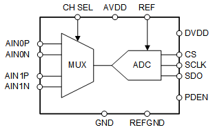
The ADS7947, ADS7948, and ADS7949 are pin-compatible 12-bit, 10-bit, and 8-bit, 2-MSPS, analog-to-digital converters (ADCs), respectively. The devices operate at a 2-MSPS sample rate with a standard 16 clock data frame. In addition, the ADS7947 (12-bit) can be operated at 2.1 MSPS, the ADS7948 (10-bit) at 2.57 MSPS, and the ADS7949 (8-bit) at 3 MSPS with a short data frame optimized for the number of clocks sufficient for conversion with no drop in performance. The devices feature both outstanding dc precision and excellent dynamic performance. This family of pin-compatible devices includes a two-channel input multiplexer and a low-power successive approximation register (SAR) ADC.
The ADS7947, ADS7948, and ADS7949 support a wide analog supply range that supports the full-scale input range up to 5 V. A simple SPI digital interface, with a digital supply that can operate as low as 1.65 V, allows for easy interfacing to a wide variety of digital controllers. Automatic power-down can be enabled when operating at slower speeds to dramatically reduce power consumption.
Offered in a tiny 3-mm × 3-mm WQFN package, the ADS7947, ADS7948, and ADS7949 are fully specified over the extended temperature range of –40°C to +125°C and are suitable for a wide variety of data acquisition applications where high performance, low power, and small size are key.
Device Information(1)
| PART NUMBER | PACKAGE | BODY SIZE (NOM) |
|---|---|---|
| ADS794x | WQFN (16) | 3.00 mm × 3.00 mm |
- For all available packages, see the orderable addendum at the end of the data sheet.
