SBAS817C November   2017  – November 2019 ADS8166 , ADS8167 , ADS8168

PRODUCTION DATA.  

  1. Features
  2. Applications
  3. Description
    1.     Device Images
      1.      ADS816x Block Diagram
  4. Revision History
  5. Pin Configuration and Functions
    1.     Pin Functions
  6. Specifications
    1. 6.1 Absolute Maximum Ratings
    2. 6.2 ESD Ratings
    3. 6.3 Recommended Operating Conditions
    4. 6.4 Thermal Information
    5. 6.5 Electrical Characteristics
    6. 6.6 Timing Requirements
    7. 6.7 Switching Characteristics
    8. 6.8 Typical Characteristics
  7. Detailed Description
    1. 7.1 Overview
    2. 7.2 Functional Block Diagram
    3. 7.3 Feature Description
      1. 7.3.1 Analog Multiplexer
        1. 7.3.1.1 Multiplexer Configurations
        2. 7.3.1.2 Multiplexer With Minimum Crosstalk
        3. 7.3.1.3 Early Switching for Direct Sensor Interface
      2. 7.3.2 Reference
        1. 7.3.2.1 Internal Reference
        2. 7.3.2.2 External Reference
      3. 7.3.3 Reference Buffer
      4. 7.3.4 REFby2 Buffer
      5. 7.3.5 Converter Module
        1. 7.3.5.1 Internal Oscillator
        2. 7.3.5.2 ADC Transfer Function
      6. 7.3.6 Low-Dropout Regulator (LDO)
    4. 7.4 Device Functional Modes
      1. 7.4.1 Channel Selection Using Internal Multiplexer
        1. 7.4.1.1 Manual Mode
        2. 7.4.1.2 On-The-Fly Mode
        3. 7.4.1.3 Auto Sequence Mode
        4. 7.4.1.4 Custom Channel Sequencing Mode
      2. 7.4.2 Digital Window Comparator
    5. 7.5 Programming
      1. 7.5.1 Data Transfer Protocols
        1. 7.5.1.1 Enhanced-SPI Interface
          1. 7.5.1.1.1 Protocols for Configuring the Device
          2. 7.5.1.1.2 Protocols for Reading From the Device
            1. 7.5.1.1.2.1 SPI Protocols With a Single SDO
            2. 7.5.1.1.2.2 SPI Protocols With Dual SDO
            3. 7.5.1.1.2.3 Clock Re-Timer Data Transfer
              1. 7.5.1.1.2.3.1 Output Bus Width Options
      2. 7.5.2 Register Read/Write Operation
    6. 7.6 Register Maps
      1. 7.6.1 Interface and Hardware Configuration Registers
        1. 7.6.1.1 REG_ACCESS Register (address = 00h) [reset = 00h]
          1. Table 11. REG_ACCESS Register Field Descriptions
        2. 7.6.1.2 PD_CNTL Register (address = 04h) [reset = 00h]
          1. Table 12. PD_CNTL Register Field Descriptions
        3. 7.6.1.3 SDI_CNTL Register (address = 008h) [reset = 00h]
          1. Table 13. SDI_CNTL Register Field Descriptions
        4. 7.6.1.4 SDO_CNTL1 Register (address = 0Ch) [reset = 00h]
          1. Table 14. SDO_CNTL1 Register Field Descriptions
        5. 7.6.1.5 SDO_CNTL2 Register (address = 0Dh) [reset = 00h]
          1. Table 15. SDO_CNTL2 Register Field Descriptions
        6. 7.6.1.6 SDO_CNTL3 Register (address = 0Eh) [reset = 00h]
          1. Table 16. SDO_CNTL3 Register Field Descriptions
        7. 7.6.1.7 SDO_CNTL4 Register (address = 0Fh) [reset = 00h]
          1. Table 17. SDO_CNTL4 Register Field Descriptions
        8. 7.6.1.8 DATA_CNTL Register (address = 10h) [reset = 00h]
          1. Table 18. DATA_CNTL Register Field Descriptions
        9. 7.6.1.9 PARITY_CNTL Register (address = 11h) [reset = 00h]
          1. Table 19. PARITY_CNTL Register Field Descriptions
      2. 7.6.2 Device Calibration Registers
        1. 7.6.2.1 OFST_CAL Register (address = 18h) [reset = 00h]
          1. Table 21. OFST_CAL Register Field Descriptions
        2. 7.6.2.2 REF_MRG1 Register (address = 19h) [reset = 00h]
          1. Table 22. REF_MRG1 Register Field Descriptions
        3. 7.6.2.3 REF_MRG2 Register (address = 1Ah) [reset = 00h]
          1. Table 24. REF_MRG2 Register Field Descriptions
        4. 7.6.2.4 REFby2_MRG Register (address = 1Bh) [reset = 00h]
          1. Table 25. REFby2_MRG Register Field Descriptions
      3. 7.6.3 Analog Input Configuration Registers
        1. 7.6.3.1 AIN_CFG Register (address = 24h) [reset = 00h]
          1. Table 28. AIN_CFG Register Field Descriptions
        2. 7.6.3.2 COM_CFG Register (address = 27h) [reset = 00h]
          1. Table 29. COM_CFG Register Field Descriptions
      4. 7.6.4 Channel Sequence Configuration Registers Map
        1. 7.6.4.1 DEVICE_CFG Register (address = 1Ch) [reset = 00h]
          1. Table 31. DEVICE_CFG Register Field Descriptions
        2. 7.6.4.2 CHANNEL_ID Register (address = 1Dh) [reset = 00h]
          1. Table 33. CHANNEL_ID Register Field Descriptions
        3. 7.6.4.3 SEQ_START Register (address = 1Eh) [reset = 00h]
          1. Table 35. SEQ_START Register Field Descriptions
        4. 7.6.4.4 SEQ_ABORT Register (address = 1Fh) [reset = 00h]
          1. Table 36. SEQ_ABORT Register Field Descriptions
        5. 7.6.4.5 ON_THE_FLY_CFG Register (address = 2Ah) [reset = 00h]
          1. Table 37. ON_THE_FLY_CFG Register Field Descriptions
        6. 7.6.4.6 AUTO_SEQ_CFG1 Register (address = 80h) [reset = 00h]
          1. Table 38. AUTO_SEQ_CFG1 Register Field Descriptions
        7. 7.6.4.7 AUTO_SEQ_CFG2 Register (address = 82h) [reset = 00h]
          1. Table 39. AUTO_SEQ_CFG2 Register Field Descriptions
        8. 7.6.4.8 Custom Channel Sequencing Mode Registers
          1. 7.6.4.8.1 CCS_START_INDEX Register (address = 88h) [reset = 00h]
            1. Table 41. CCS_START_INDEX Register Field Descriptions
          2. 7.6.4.8.2 CCS_END_INDEX Register (address = 89h) [reset = 00h]
            1. Table 42. CCS_END_INDEX Register Field Descriptions
          3. 7.6.4.8.3 CCS_SEQ_LOOP Register (address = 8Bh) [reset = 00h]
            1. Table 43. CCS_SEQ_LOOP Register Field Descriptions
          4. 7.6.4.8.4 CCS_CHID_INDEX_m Registers (address = 8C, 8E, 90, 92, 94, 96, 98, 9A, 9C, 9E, A0, A2, A4, A6, A8, and AAh) [reset = 00h]
            1. Table 44. CCS_CHID_INDEX_m Register Field Descriptions
          5. 7.6.4.8.5 REPEAT_INDEX_m Registers (address = 8D, 8F, 91, 93, 95, 97, 99, 9B, 9D, 9F, A1, A3, A5, A7, A9, and ABh) [reset = 00h]
            1. Table 45. REPEAT_INDEX_m Register Field Descriptions
      5. 7.6.5 Digital Window Comparator Configuration Registers Map
        1. 7.6.5.1  ALERT_CFG Register (address = 2Eh) [reset = 00h]
          1. Table 47. ALERT_CFG Register Field Descriptions
        2. 7.6.5.2  HI_TRIG_AINx[15:0] Register (address = 4Dh to 30h) [reset = 0000h]
          1. Table 49. HI_TRIG_AINx[15:0] Registers Field Descriptions
        3. 7.6.5.3  LO_TRIG_AINx[15:0] Register (address = 71h to 54h) [reset = 0000h]
          1. Table 51. LO_TRIG_AINx[15:0] Registers Field Descriptions
        4. 7.6.5.4  HYSTERESIS_AINx[7:0] Register (address = 4Fh to 33h) [reset = 00h]
          1. Table 52. HYSTERESIS_AINx[7:0] Register Field Descriptions
        5. 7.6.5.5  ALERT_LO_STATUS Register (address = 78h) [reset = 00h]
          1. Table 53. ALERT_LO_STATUS Register Field Descriptions
        6. 7.6.5.6  ALERT_HI_STATUS Register (address = 79h) [reset = 00h]
          1. Table 54. ALERT_HI_STATUS Register Field Descriptions
        7. 7.6.5.7  ALERT_STATUS Register (address = 7Ah) [reset = 00h]
          1. Table 55. ALERT_STATUS Register Field Descriptions
        8. 7.6.5.8  CURR_ALERT_LO_STATUS Register (address = 7Ch) [reset = 00h]
          1. Table 56. CURR_ALERT_LO_STATUS Register Field Descriptions
        9. 7.6.5.9  CURR_ALERT_HI_STATUS Register (address = 7Dh) [reset = 00h]
          1. Table 57. CURR_ALERT_HI_STATUS Register Field Descriptions
        10. 7.6.5.10 CURR_ALERT_STATUS Register (address = 7Eh) [reset = 00h]
          1. Table 58. CURR_ALERT_STATUS Register Field Descriptions
  8. Application and Implementation
    1. 8.1 Application Information
      1. 8.1.1 Multiplexer Input Connection
      2. 8.1.2 Selecting an ADC Input Buffer
    2. 8.2 Typical Applications
      1. 8.2.1 1-MSPS DAQ Circuit With Lowest Distortion and Noise Performance
        1. 8.2.1.1 Design Requirements
        2. 8.2.1.2 Detailed Design Procedure
        3. 8.2.1.3 Application Curve
      2. 8.2.2 8-Channel Photodiode Detector With Smallest Size and Lowest Number of Components
        1. 8.2.2.1 Design Requirements
        2. 8.2.2.2 Detailed Design Procedure
      3. 8.2.3 1-MSPS DAQ Circuit for Factory Automation
        1. 8.2.3.1 Design Requirements
        2. 8.2.3.2 Detailed Design Procedure
  9. Power Supply Recommendations
  10. 10Layout
    1. 10.1 Layout Guidelines
      1. 10.1.1 Analog Signal Path
      2. 10.1.2 Grounding and PCB Stack-Up
      3. 10.1.3 Decoupling of Power Supplies
      4. 10.1.4 Reference Decoupling
      5. 10.1.5 Reference Buffer Decoupling
      6. 10.1.6 Multiplexer Input Decoupling
      7. 10.1.7 ADC Input Decoupling
      8. 10.1.8 Example Schematic
    2. 10.2 Layout Example
  11. 11Device and Documentation Support
    1. 11.1 Documentation Support
      1. 11.1.1 Related Documentation
    2. 11.2 Related Links
    3. 11.3 Receiving Notification of Documentation Updates
    4. 11.4 Community Resources
    5. 11.5 Trademarks
    6. 11.6 Electrostatic Discharge Caution
    7. 11.7 Glossary
  12. 12Mechanical, Packaging, and Orderable Information

Package Options

Mechanical Data (Package|Pins)
Thermal pad, mechanical data (Package|Pins)
Orderable Information

Early Switching for Direct Sensor Interface

Figure 33 shows the small-signal equivalent model of the ADS816x analog inputs. The multiplexer input has a switch resistance (RMUX) and parasitic capacitance (CMUX). The parasitic capacitance causes a charge kickback on the MUX analog input at the same time as the ADC sampling capacitor causes a charge kickback on ADC inputs.

ADS8166 ADS8167 ADS8168 enhanced_settling_time_bd.gifFigure 33. Synchronous and Timed Switching of the MUX and ADC Input Switches

In conventional multichannel SAR ADCs, the acquisition time of the ADC is also the settling time available at the analog inputs of the multiplexer because these times are internally connected. Thus, high-bandwidth op amps are required at the analog inputs of the multiplexer to settle the charge kickback. However, multiple high-bandwidth op amps significantly increase power dissipation, cost, and size of the solution.

The analog inputs of the ADS816x provide a long settling time (tCYCLE – 100 ns), resulting in long acquisition time at the MUX inputs when using a driver amplifier between the MUX outputs and the ADC inputs. Figure 34 shows a timing diagram of this long acquisition phase. The low parasitic capacitance together with the enhanced settling time eliminate the need to use an op amp at the multiplexer input in most applications.
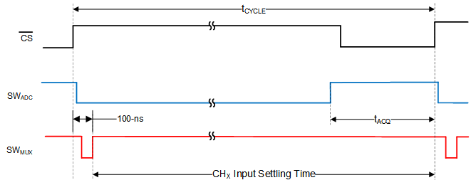
ADS8166 ADS8167 ADS8168 enhanced-_settling_time_details.gifFigure 34. Early Switching of the MUX Enables a Long Acquisition Phase

Averaging several output codes of a particular MUX input channel without switching the MUX achieves better accuracy and noise performance. The output of the multiplexer does not create a charge kickback as long as SDI is set to 0 (that is, as long as SDI returns the NOP command); see Figure 43 and Figure 45. The multiplexer does not switch during subsequent conversions except for the first time when a channel is selected. Thus high-impedance sources (such as the voltage from the resistor dividers) can be connected to the analog inputs of the multiplexer without an op amp.