SBAS817C November 2017 – November 2019 ADS8166 , ADS8167 , ADS8168
PRODUCTION DATA.
- 1 Features
- 2 Applications
- 3 Description
- 4 Revision History
- 5 Pin Configuration and Functions
- 6 Specifications
-
7 Detailed Description
- 7.1 Overview
- 7.2 Functional Block Diagram
- 7.3 Feature Description
- 7.4 Device Functional Modes
- 7.5 Programming
- 7.6
Register Maps
- 7.6.1
Interface and Hardware Configuration Registers
- 7.6.1.1 REG_ACCESS Register (address = 00h) [reset = 00h]
- 7.6.1.2 PD_CNTL Register (address = 04h) [reset = 00h]
- 7.6.1.3 SDI_CNTL Register (address = 008h) [reset = 00h]
- 7.6.1.4 SDO_CNTL1 Register (address = 0Ch) [reset = 00h]
- 7.6.1.5 SDO_CNTL2 Register (address = 0Dh) [reset = 00h]
- 7.6.1.6 SDO_CNTL3 Register (address = 0Eh) [reset = 00h]
- 7.6.1.7 SDO_CNTL4 Register (address = 0Fh) [reset = 00h]
- 7.6.1.8 DATA_CNTL Register (address = 10h) [reset = 00h]
- 7.6.1.9 PARITY_CNTL Register (address = 11h) [reset = 00h]
- 7.6.2 Device Calibration Registers
- 7.6.3 Analog Input Configuration Registers
- 7.6.4
Channel Sequence Configuration Registers Map
- 7.6.4.1 DEVICE_CFG Register (address = 1Ch) [reset = 00h]
- 7.6.4.2 CHANNEL_ID Register (address = 1Dh) [reset = 00h]
- 7.6.4.3 SEQ_START Register (address = 1Eh) [reset = 00h]
- 7.6.4.4 SEQ_ABORT Register (address = 1Fh) [reset = 00h]
- 7.6.4.5 ON_THE_FLY_CFG Register (address = 2Ah) [reset = 00h]
- 7.6.4.6 AUTO_SEQ_CFG1 Register (address = 80h) [reset = 00h]
- 7.6.4.7 AUTO_SEQ_CFG2 Register (address = 82h) [reset = 00h]
- 7.6.4.8
Custom Channel Sequencing Mode Registers
- 7.6.4.8.1 CCS_START_INDEX Register (address = 88h) [reset = 00h]
- 7.6.4.8.2 CCS_END_INDEX Register (address = 89h) [reset = 00h]
- 7.6.4.8.3 CCS_SEQ_LOOP Register (address = 8Bh) [reset = 00h]
- 7.6.4.8.4 CCS_CHID_INDEX_m Registers (address = 8C, 8E, 90, 92, 94, 96, 98, 9A, 9C, 9E, A0, A2, A4, A6, A8, and AAh) [reset = 00h]
- 7.6.4.8.5 REPEAT_INDEX_m Registers (address = 8D, 8F, 91, 93, 95, 97, 99, 9B, 9D, 9F, A1, A3, A5, A7, A9, and ABh) [reset = 00h]
- 7.6.5
Digital Window Comparator Configuration Registers Map
- 7.6.5.1 ALERT_CFG Register (address = 2Eh) [reset = 00h]
- 7.6.5.2 HI_TRIG_AINx[15:0] Register (address = 4Dh to 30h) [reset = 0000h]
- 7.6.5.3 LO_TRIG_AINx[15:0] Register (address = 71h to 54h) [reset = 0000h]
- 7.6.5.4 HYSTERESIS_AINx[7:0] Register (address = 4Fh to 33h) [reset = 00h]
- 7.6.5.5 ALERT_LO_STATUS Register (address = 78h) [reset = 00h]
- 7.6.5.6 ALERT_HI_STATUS Register (address = 79h) [reset = 00h]
- 7.6.5.7 ALERT_STATUS Register (address = 7Ah) [reset = 00h]
- 7.6.5.8 CURR_ALERT_LO_STATUS Register (address = 7Ch) [reset = 00h]
- 7.6.5.9 CURR_ALERT_HI_STATUS Register (address = 7Dh) [reset = 00h]
- 7.6.5.10 CURR_ALERT_STATUS Register (address = 7Eh) [reset = 00h]
- 7.6.1
Interface and Hardware Configuration Registers
- 8 Application and Implementation
- 9 Power Supply Recommendations
- 10Layout
- 11Device and Documentation Support
- 12Mechanical, Packaging, and Orderable Information
Package Options
Mechanical Data (Package|Pins)
- RHB|32
Thermal pad, mechanical data (Package|Pins)
- RHB|32
Orderable Information
8.1.1 Multiplexer Input Connection
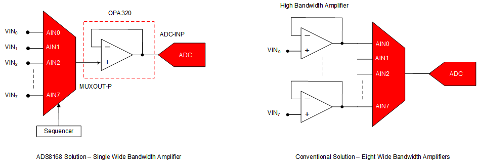
Conventional multichannel ADC solutions internally connect the multiplexer output directly to the switched capacitor input of the ADC. Conventionally, a wide bandwidth amplifier is required for each channel. For the ADS816x, only one amplifier is required for many applications. The ADS816x solution shown in Figure 98 has lower power, a smaller PCB area, and lower cost compared to the comparative solution. Furthermore, from a calibration perspective, the offset error in the ADS816x solution is the same in each channel and is set by the multiplexer output amplifier. The offset error in the conventional solution, on the other hand, is different for each channel. Calibrating the offset error for the conventional solution also requires a separate calibration for each channel.
 Figure 98. Small-Size and Low-Power 8-Channel DAQ System Using the ADS816x
 When connecting the sensor directly to the input of the ADS816x, the maximum switching speed of the multiplexer is limited by multiplexer on-resistance and parasitic capacitance. Figure 99 illustrates the source resistance (RS0, RS1…), multiplexer impedance (RMUX), multiplexer capacitance (CMUX), op amp input capacitance (COPA), and the stray PCB capacitance at the output of the multiplexer (CSTRAY). In this example, the total output capacitance is the combination of the multiplexer output capacitance, the op amp input capacitance, and the stray capacitance (CMUX + COPA + CSTRAY) = 15 pF. When switching to a channel, this capacitance must be charged to the sensor output voltage via the source resistance and the multiplexer resistance (RS0 + RMUX).
Equation 2 can be used to estimate the number of time constants required for N bits of settling. For this example, to achieve 16-bit settling, 11.09 time constants are required. Thus, as computed in Equation 3 and Equation 4, for channel 0 the required settling time is 167 ns.
 Figure 99. Direct Sensor Interface With the ADS816x in an 8-Channel, Single-Ended Configuration
 When operating at 1 MSPS in either manual mode, auto sequence mode, or custom channel sequencing mode, a 900-ns settling time is available at the analog inputs of the multiplexer; see the Early Switching for Direct Sensor Interface section. Using Equation 4, the maximum sensor output impedance for a direct connection is 5.4 kΩ.
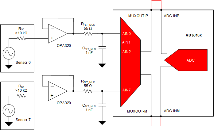
In some applications, such as temperature sensing, the sensor output impedance can be greater than 10 kΩ. When scanning the multiplexer channels at high throughput, the relatively higher driving impedance results in a settling error. In such cases, Figure 100 shows that the multiplexer inputs can be driven using an amplifier. The multiplexer outputs can be connected to the ADC inputs directly. For best distortion performance, an amplifier can be used between the multiplexer and the ADC as described in the Selecting an ADC Input Buffer section.
 Figure 100. High Output Impedance Sensor Interface