SBAS779B December 2016 – March 2021 ADS8671 , ADS8675
PRODUCTION DATA
- 1 Features
- 2 Applications
- 3 Description
- 4 Revision History
- 5 Pin Configuration and Functions
-
6 Specifications
- 6.1 Absolute Maximum Ratings
- 6.2 ESD Ratings
- 6.3 Recommended Operating Conditions
- 6.4 Thermal Information
- 6.5 Electrical Characteristics
- 6.6 Timing Requirements: Conversion Cycle
- 6.7 Timing Requirements: Asynchronous Reset
- 6.8 Timing Requirements: SPI-Compatible Serial Interface
- 6.9 Timing Requirements: Source-Synchronous Serial Interface (External Clock)
- 6.10 Timing Requirements: Source-Synchronous Serial Interface (Internal Clock)
- 6.11 Timing Diagrams
- 6.12 Typical Characteristics
-
7 Detailed Description
- 7.1 Overview
- 7.2 Functional Block Diagram
- 7.3 Feature Description
- 7.4 Device Functional Modes
- 7.5 Programming
- 7.6
Register Maps
- 7.6.1
Device Configuration and Register Maps
- 7.6.1.1 DEVICE_ID_REG Register (address = 00h)
- 7.6.1.2 RST_PWRCTL_REG Register (address = 04h)
- 7.6.1.3 SDI_CTL_REG Register (address = 08h)
- 7.6.1.4 SDO_CTL_REG Register (address = 0Ch)
- 7.6.1.5 DATAOUT_CTL_REG Register (address = 10h)
- 7.6.1.6 RANGE_SEL_REG Register (address = 14h)
- 7.6.1.7 ALARM_REG Register (address = 20h)
- 7.6.1.8 ALARM_H_TH_REG Register (address = 24h)
- 7.6.1.9 ALARM_L_TH_REG Register (address = 28h)
- 7.6.1
Device Configuration and Register Maps
- 8 Application and Implementation
- 9 Power Supply Recommendations
- 10Layout
- 11Device and Documentation Support
Package Options
Mechanical Data (Package|Pins)
- PW|16
Thermal pad, mechanical data (Package|Pins)
Orderable Information
7.3.3 Input Protection Circuit
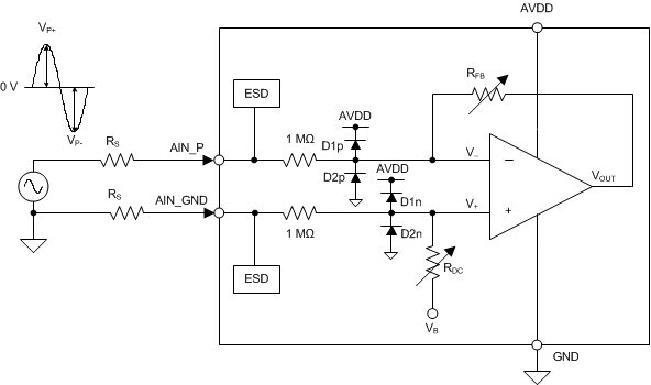
The device features an internal overvoltage protection (OVP) circuit on each of the analog inputs. Use the internal protection circuit only as a secondary protection scheme. The external protection devices in the end application are highly recommended to be used to protect against surges, electrostatic discharge (ESD), and electrical fast transient (EFT) conditions. A conceptual block diagram of the internal OVP circuit is shown in Figure 7-2.
 Figure 7-2 Input Overvoltage Protection Circuit Schematic
As shown in Figure 7-2, the combination of the 1-MΩ (or, 1.2 MΩ for appropriate input ranges) input resistors along with the PGA gain-setting resistors RFB and RDC limit the current flowing into the input pin. A combination of anti-parallel diodes, D1 and D2 are added to protect the internal circuitry and set the overvoltage protection limits.
Table 7-1 explains the various operating conditions for the device when powered on. This table indicates that when the device is properly powered up (AVDD = 5 V) or offers a low impedance of < 30 kΩ, the internal overvoltage protection circuit can withstand up to ±20 V on the analog input pins.
| INPUT CONDITION (VOVP = ±20 V) | TEST CONDITION | ADC OUTPUT | COMMENTS | |
|---|---|---|---|---|
| CONDITION | RANGE | |||
| |VIN| < |VRANGE| | Within operating range | All input ranges | Valid | Device functions as per data sheet specifications. |
| |VRANGE| < |VIN| < |VOVP| | Beyond operating range but within overvoltage range | All input ranges | Saturated | ADC output is saturated, but device is internally protected (not recommended for extended time). |
| |VIN| > |VOVP| | Beyond overvoltage range | All input ranges | Saturated | This usage condition can cause irreversible damage to the device. |
The results indicated in Table 7-1 are based on an assumption that the analog input pin is driven by a very low impedance source (RS is approximately 0 Ω). However, if the source driving the input has higher impedance, the current flowing through the protection diodes reduces further, thereby increasing the OVP voltage range. Higher source impedances result in gain errors and contribute to overall system noise performance.
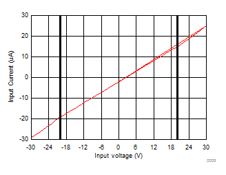
Figure 7-3 shows the voltage versus current response of the internal overvoltage protection circuit when the device is powered on. According to this current-to-voltage (I-V) response, the current flowing into the device input pin is limited by the 1-MΩ (or 1.2 MΩ for appropriate input ranges) input impedance. However, for voltages beyond ±20 V, the internal node voltages surpass the break-down voltage for internal transistors, thus setting the limit for overvoltage protection on the input pin.
The same overvoltage protection circuit also provides protection to the device when the device is not powered on and AVDD is floating. This condition can arise when the input signals are applied before the ADC is fully powered on. The overvoltage protection limits for this condition are shown in Table 7-2.
| INPUT CONDITION (VOVP = ±15 V) | TEST CONDITION | ADC OUTPUT | COMMENTS | |
|---|---|---|---|---|
| CONDITION | RANGE | |||
| |VIN| < |VOVP| | Within overvoltage range | All input ranges | Invalid | Device is not functional but is protected internally by the OVP circuit. |
| |VIN| > |VOVP| | Beyond overvoltage range | All input ranges | Invalid | This usage condition can cause irreversible damage to the device. |
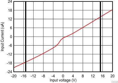
Figure 7-4 shows the I-V response of the internal overvoltage protection circuit when the device is not powered on. According to this I-V response, the current flowing into the device input pin is limited by the 1-MΩ input impedance. However, for voltages beyond ±15 V, the internal node voltage surpasses the break-down voltage for internal transistors, thus setting the limit for overvoltage protection on the input pin.
 Figure 7-3 I-V Curve for the Input OVP Circuit (AVDD = 5 V)
  Figure 7-4 I-V Curve for the Input OVP Circuit (AVDD = Floating)