SBAS779B December 2016 – March 2021 ADS8671 , ADS8675
PRODUCTION DATA
- 1 Features
- 2 Applications
- 3 Description
- 4 Revision History
- 5 Pin Configuration and Functions
-
6 Specifications
- 6.1 Absolute Maximum Ratings
- 6.2 ESD Ratings
- 6.3 Recommended Operating Conditions
- 6.4 Thermal Information
- 6.5 Electrical Characteristics
- 6.6 Timing Requirements: Conversion Cycle
- 6.7 Timing Requirements: Asynchronous Reset
- 6.8 Timing Requirements: SPI-Compatible Serial Interface
- 6.9 Timing Requirements: Source-Synchronous Serial Interface (External Clock)
- 6.10 Timing Requirements: Source-Synchronous Serial Interface (Internal Clock)
- 6.11 Timing Diagrams
- 6.12 Typical Characteristics
-
7 Detailed Description
- 7.1 Overview
- 7.2 Functional Block Diagram
- 7.3 Feature Description
- 7.4 Device Functional Modes
- 7.5 Programming
- 7.6
Register Maps
- 7.6.1
Device Configuration and Register Maps
- 7.6.1.1 DEVICE_ID_REG Register (address = 00h)
- 7.6.1.2 RST_PWRCTL_REG Register (address = 04h)
- 7.6.1.3 SDI_CTL_REG Register (address = 08h)
- 7.6.1.4 SDO_CTL_REG Register (address = 0Ch)
- 7.6.1.5 DATAOUT_CTL_REG Register (address = 10h)
- 7.6.1.6 RANGE_SEL_REG Register (address = 14h)
- 7.6.1.7 ALARM_REG Register (address = 20h)
- 7.6.1.8 ALARM_H_TH_REG Register (address = 24h)
- 7.6.1.9 ALARM_L_TH_REG Register (address = 28h)
- 7.6.1
Device Configuration and Register Maps
- 8 Application and Implementation
- 9 Power Supply Recommendations
- 10Layout
- 11Device and Documentation Support
Package Options
Mechanical Data (Package|Pins)
- PW|16
Thermal pad, mechanical data (Package|Pins)
Orderable Information
7.4.1.3 Multiple Devices: Daisy-Chain Topology
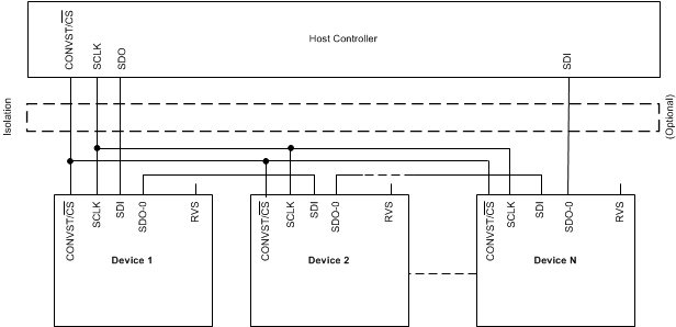
A typical connection diagram showing multiple devices in a daisy-chain topology is shown in Figure 7-22.
 Figure 7-22 Daisy-Chain Connection Schematic
The CONVST/CS and SCLK inputs of all devices are connected together and controlled by a single CONVST/CS and SCLK pin of the host controller, respectively. The SDI input pin of the first device in the chain (device 1) is connected to the SDO-x pin of the host controller, the SDO-0 output pin of device 1 is connected to the SDI input pin of device 2, and so forth. The SDO-0 output pin of the last device in the chain (device N) is connected to the SDI pin of the host controller.
To operate multiple devices in a daisy-chain topology, the host controller must program the configuration registers in each device with identical values. The devices must operate with a single SDO-0 output, using the external clock with any of the legacy, SPI-compatible protocols for data read and data write operations. In the SDO_CTL_REG register, bits 7-0 must be programmed to 00h.
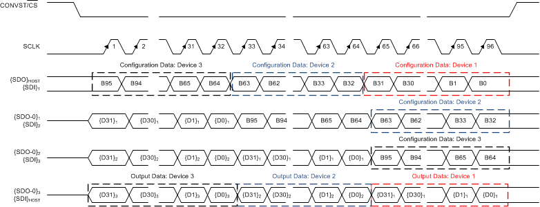
All devices in the daisy-chain topology sample their analog input signals on the rising edge of the CONVST/CS signal and the data transfer frame starts with a falling edge of the same signal. At the launch edge of the SCLK signal, every device in the chain shifts out the MSB to the SDO-0 pin. On every SCLK capture edge, each device in the chain shifts in data received on its SDI pin as the LSB bit of the unified shift register; see Figure 7-19. Therefore, in a daisy-chain configuration, the host controller receives the data of device N, followed by the data of device N-1, and so forth (in MSB-first fashion). On the rising edge of the CONVST/CS signal, each device decodes the contents in its unified and takes appropriate action.
For N devices connected in a daisy-chain topology, an optimal data transfer frame must contain 32 × N SCLK capture edges (see Figure 7-23). A shorter data transfer frame can result in an erroneous device configuration and must be avoided. For a data transfer frame with > 32 × N SCLK capture edges, the host controller must appropriately align the configuration data for each device before bringing CONVST/CS high.
The overall throughput of the system is proportionally reduced with the number of devices connected in a daisy-chain topology.
A typical timing diagram for three devices connected in a daisy-chain topology and using the SPI-00-S protocol is shown in Figure 7-23.
 Figure 7-23 Three Devices in Daisy-Chain Mode Timing Diagram