SBAS779B December 2016 – March 2021 ADS8671 , ADS8675
PRODUCTION DATA
- 1 Features
- 2 Applications
- 3 Description
- 4 Revision History
- 5 Pin Configuration and Functions
-
6 Specifications
- 6.1 Absolute Maximum Ratings
- 6.2 ESD Ratings
- 6.3 Recommended Operating Conditions
- 6.4 Thermal Information
- 6.5 Electrical Characteristics
- 6.6 Timing Requirements: Conversion Cycle
- 6.7 Timing Requirements: Asynchronous Reset
- 6.8 Timing Requirements: SPI-Compatible Serial Interface
- 6.9 Timing Requirements: Source-Synchronous Serial Interface (External Clock)
- 6.10 Timing Requirements: Source-Synchronous Serial Interface (Internal Clock)
- 6.11 Timing Diagrams
- 6.12 Typical Characteristics
-
7 Detailed Description
- 7.1 Overview
- 7.2 Functional Block Diagram
- 7.3 Feature Description
- 7.4 Device Functional Modes
- 7.5 Programming
- 7.6
Register Maps
- 7.6.1
Device Configuration and Register Maps
- 7.6.1.1 DEVICE_ID_REG Register (address = 00h)
- 7.6.1.2 RST_PWRCTL_REG Register (address = 04h)
- 7.6.1.3 SDI_CTL_REG Register (address = 08h)
- 7.6.1.4 SDO_CTL_REG Register (address = 0Ch)
- 7.6.1.5 DATAOUT_CTL_REG Register (address = 10h)
- 7.6.1.6 RANGE_SEL_REG Register (address = 14h)
- 7.6.1.7 ALARM_REG Register (address = 20h)
- 7.6.1.8 ALARM_H_TH_REG Register (address = 24h)
- 7.6.1.9 ALARM_L_TH_REG Register (address = 28h)
- 7.6.1
Device Configuration and Register Maps
- 8 Application and Implementation
- 9 Power Supply Recommendations
- 10Layout
- 11Device and Documentation Support
Package Options
Mechanical Data (Package|Pins)
- PW|16
Thermal pad, mechanical data (Package|Pins)
Orderable Information
3 Description
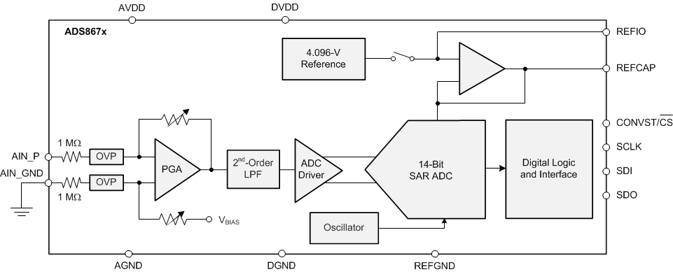
The ADS8671 and ADS8675 belong to a family of integrated data acquisition system based on a successive approximation (SAR) analog-to-digital converter (ADC). The devices feature a high-speed, high-precision SAR ADC, integrated analog front-end (AFE) input driver circuit, overvoltage protection circuit up to ±20 V, and an on-chip 4.096-V reference with extremely low temperature drift.
The devices operate on a single 5-V analog supply, but support true bipolar input ranges of ±12.288 V, ±6.144 V, ±10.24 V, ±5.12 V, and ±2.56 V, as well as unipolar input ranges of 0 V to 12.288 V, 0 V to 10.24 V, 0 V to 6.144 V, and 0 V to 5.12 V. The gain and offset errors are accurately trimmed within the specified values for each input range to ensure high dc precision. The input range selection is done by software programming of the device internal registers. The devices offer a high resistive input impedance (≥ 1 MΩ) irrespective of the selected input range.
The multiSPI digital interface is backward-compatible to the traditional SPI protocol. Additionally, configurable features simplify interface to a wide range of host controllers.
| PART NUMBER | PACKAGE | BODY SIZE (NOM) |
|---|---|---|
| ADS866x | TSSOP (16) | 5.00 mm × 4.40 mm |
 Block
Diagram