SBOS927B May 2019 – October 2021 ALM2402F-Q1
PRODUCTION DATA
- 1 Features
- 2 Applications
- 3 Description
- 4 Revision History
- 5 Pin Configuration and Functions
- 6 Specifications
- 7 Detailed Description
- 8 Application and Implementation
- 9 Power Supply Recommendations
- 10Layout
- 11Device and Documentation Support
- 12Mechanical, Packaging, and Orderable Information
Package Options
Mechanical Data (Package|Pins)
- PWP|14
Thermal pad, mechanical data (Package|Pins)
- PWP|14
Orderable Information
3 Description
The ALM2402F-Q1 is a dual-power op amp with features and performance that make this device preferable for resolver-based automotive applications. The high gain bandwidth and slew rate of the device, along with a continuous high-output current-drive capability, make this device an excellent choice to provide a low distortion and differential high amplitude excitation required for modern resolvers. Current limiting and overtemperature detection enhance overall system robustness when driving analog signals over wires that are susceptible to faults.
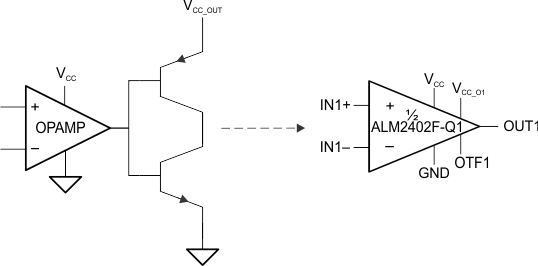
The ALM2402F-Q1 rail-to-rail output, enabled by the low Rds(on) PMOS and NMOS transistors, keeps the power dissipation low. The small HTSSOP package with thermal pad and low RθJA allows users to deliver high currents to loads while minimizing board space. This minimized board space is one of the key advantages offered by the ALM2402F-Q1 when used in modern hybrid and electric vehicles.
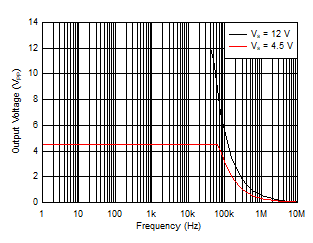
The ALM2402F-Q1 maximum output voltage is determined using the Maximum Output Voltage vs Frequency plot at the bottom of this page.
| PART NUMBER | PACKAGE | BODY SIZE (NOM) |
|---|---|---|
| ALM2402F-Q1 | HTSSOP (14) | 5.00 mm × 4.40 mm |
 Simplified Schematic
 Maximum Output Voltage vs
Frequency