SBOSA37A November 2020 – March 2023 ALM2403-Q1
PRODUCTION DATA
- 1 Features
- 2 Applications
- 3 Description
- 4 Revision History
- 5 Pin Configuration and Functions
- 6 Specifications
- 7 Detailed Description
- 8 Application and Implementation
- 9 Device and Documentation Support
- 10Mechanical, Packaging, and Orderable Information
Package Options
Mechanical Data (Package|Pins)
- PWP|14
Thermal pad, mechanical data (Package|Pins)
- PWP|14
Orderable Information
8.2 Typical Application
High-power ac and brushless dc (BLDC) motor-drive applications need position feedback to efficiently and accurately drive the motor. Position feedback can be achieved by using optical encoders, hall sensors, or resolvers. Resolvers are the main choice when environmental or longevity requirements are challenging and extensive.
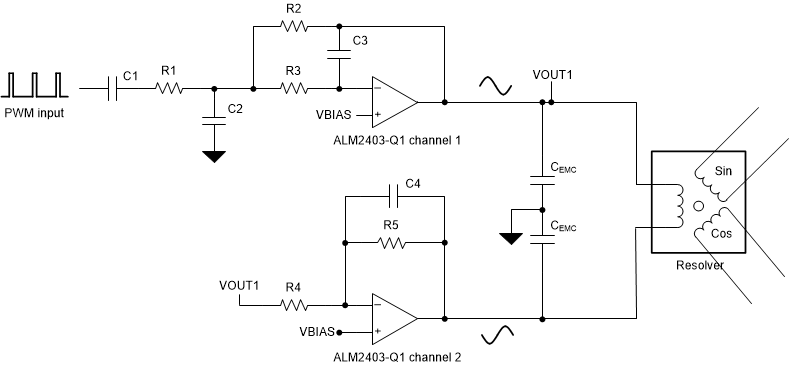
A resolver acts as a transformer with one primary coil and two secondary coils. The primary coil, or excitation coil, is located on the rotor of the resolver. As the rotor of the resolver spins, the excitation coil induces a current into the sine and cosine sensing coils. These coils are oriented 90 degrees from one another, and the voltage from the sine and cosine coils is translated into a vector position by the microcontroller or resolver-to-digital converter chip.
Resolver excitation coils can have a very low dc resistance (< 100 Ω), requiring a sink and a source of up to 200 mA from the excitation driver. The ALM2403-Q1 can source and sink this current while providing current-limiting and thermal-shutdown protection. Incorporating these protections in a resolver design can increase the life of the end product.
The input to the ALM2403-Q1 can be an analog sine wave generated by the resolver-to-digital converter chip or a pulse-width modulation (PWM) signal generated from a microcontroller I/O pin. In the case of the latter, a filter stage is needed to extract a lower bandwidth sine wave from the PWM signal. This sine wave would then be the input signal to the ALM2403-Q1. As a result of high gain bandwidth, the ALM2403-Q1 can be configured as a filter stage while providing the required output drive. This configuration significantly reduces the total solution size and design complexity of the resolver-drive signal chain. The fundamental design steps to achieve this functionality are shown in this application example, and can be applied to other inductive-load applications as well.
 Figure 8-2 Resolver-Based Application