SBOSA37A November   2020  – March 2023 ALM2403-Q1

PRODUCTION DATA  

  1. Features
  2. Applications
  3. Description
  4. Revision History
  5. Pin Configuration and Functions
  6. Specifications
    1. 6.1 Absolute Maximum Ratings
    2. 6.2 ESD Ratings
    3. 6.3 Recommended Operating Conditions
    4. 6.4 Thermal Information
    5. 6.5 Electrical Characteristics
    6. 6.6 Typical Characteristics
  7. Detailed Description
    1. 7.1 Overview
    2. 7.2 Functional Block Diagram
    3. 7.3 Feature Description
      1. 7.3.1 Overtemperature and Shutdown Pin (OTF/SH_DN)
      2. 7.3.2 Thermal Shutdown
      3. 7.3.3 Current-Limit and Short-Circuit Protection
      4. 7.3.4 Input Common-Mode Range
      5. 7.3.5 Reverse Body Diodes in Output-Stage Transistors
      6. 7.3.6 EMI Filtering
    4. 7.4 Device Functional Modes
      1. 7.4.1 Open-Loop and Closed-Loop Operation
      2. 7.4.2 Shutdown
  8. Application and Implementation
    1. 8.1 Application Information
      1. 8.1.1 Capacitive Load and Stability
    2. 8.2 Typical Application
      1. 8.2.1 Design Requirements
      2. 8.2.2 Detailed Design Procedure
        1. 8.2.2.1 Resolver Excitation Amplifier Combined With MFB 2nd-Order, Low-Pass Filter
          1. 8.2.2.1.1 Filter Design
          2. 8.2.2.1.2 Short-to-Battery Protection
        2. 8.2.2.2 Power Dissipation and Thermal Reliability
          1. 8.2.2.2.1 Improving Package Thermal Performance
      3. 8.2.3 Application Curves
    3. 8.3 Power Supply Recommendations
    4. 8.4 Layout
      1. 8.4.1 Layout Guidelines
      2. 8.4.2 Layout Example
  9. Device and Documentation Support
    1. 9.1 Documentation Support
      1. 9.1.1 Related Documentation
    2. 9.2 Receiving Notification of Documentation Updates
    3. 9.3 Support Resources
    4. 9.4 Trademarks
    5. 9.5 Electrostatic Discharge Caution
    6. 9.6 Glossary
  10. 10Mechanical, Packaging, and Orderable Information

Package Options

Mechanical Data (Package|Pins)
Thermal pad, mechanical data (Package|Pins)
Orderable Information

Resolver Excitation Amplifier Combined With MFB 2nd-Order, Low-Pass Filter

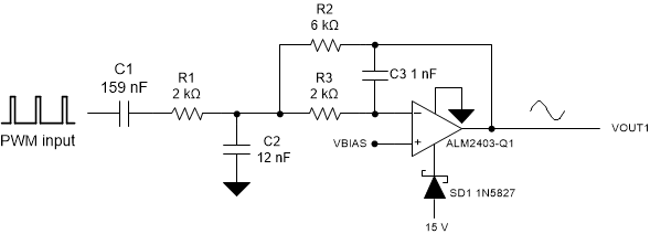
GUID-20201109-CA0I-CZWB-MWRZ-LDB8LKMJTRZD-low.gif Figure 8-3 Two-Pole MFB Filter

When designing a low-pass filter, the most important design criteria is to decide the corner frequency. In this design example, the resolver excitation frequency is 10 kHz and PWM frequency is 320 kHz. Thus, we want to make sure that the low-pass filter corner frequency is greater than 10 kHz, and there is maximum attenuation of harmonic interference generated from the PWM signal. Figure 8-3 shows a single channel of the ALM2403-Q1 configured as a 2-pole multiple feedback (MFB) filter with a –40 dB/decade rolloff. The MFB topology enables a steep rolloff while reducing BOM count. The output from this circuit is a sine wave that can then be inverted using the second channel of the ALM2403-Q1; see Figure 8-2. Thus, both ALM2403-Q1 channels combined provide the required resolver excitation signal.