SPRSP65F April   2021  – January 2023 AM2431 , AM2432 , AM2434

PRODUCTION DATA  

  1. Features
  2. Applications
  3. Description
    1. 3.1 Functional Block Diagram
  4. Revision History
  5. Device Comparison
    1. 5.1 Related Products
  6. Terminal Configuration and Functions
    1. 6.1 Pin Diagram
      1. 6.1.1 AM243x ALV Pin Diagram
      2. 6.1.2 AM243x ALX Pin Diagram
    2. 6.2 Pin Attributes
      1.      13
      2.      14
      3. 6.2.1 AM243x Package Comparison Table (ALV vs. ALX)
    3. 6.3 Signal Descriptions
      1.      17
      2. 6.3.1  AM243x_ALX Package - Unsupported Interfaces and Signals
      3. 6.3.2  ADC
        1.       MAIN Domain Instances
          1.        21
      4. 6.3.3  CPSW
        1.       MAIN Domain Instances
          1.        24
          2.        25
          3.        26
          4.        27
          5. 6.3.3.1.1 CPSW3G IOSETs
      5. 6.3.4  CPTS
        1.       MAIN Domain Instances
          1.        31
          2.        32
      6. 6.3.5  DDRSS
        1.       MAIN Domain Instances
          1.        35
      7. 6.3.6  ECAP
        1.       MAIN Domain Instances
          1.        38
          2.        39
          3.        40
      8. 6.3.7  Emulation and Debug
        1.       MAIN Domain Instances
          1.        43
        2.       MCU Domain Instances
          1.        45
      9. 6.3.8  EPWM
        1.       MAIN Domain Instances
          1.        48
          2.        49
          3.        50
          4.        51
          5.        52
          6.        53
          7.        54
          8.        55
          9.        56
          10.        57
      10. 6.3.9  EQEP
        1.       MAIN Domain Instances
          1.        60
          2.        61
          3.        62
      11. 6.3.10 FSI
        1.       MAIN Domain Instances
          1.        65
          2.        66
          3.        67
          4.        68
          5.        69
          6.        70
          7.        71
          8.        72
      12. 6.3.11 GPIO
        1.       MAIN Domain Instances
          1.        75
          2.        76
        2.       MCU Domain Instances
          1.        78
      13. 6.3.12 GPMC
        1.       MAIN Domain Instances
          1.        81
          2. 6.3.12.1.1 GPMC0 IOSETs (ALV)
      14. 6.3.13 I2C
        1.       MAIN Domain Instances
          1.        85
          2.        86
          3.        87
          4.        88
        2.       MCU Domain Instances
          1.        90
          2.        91
      15. 6.3.14 MCAN
        1.       MAIN Domain Instances
          1.        94
          2.        95
      16. 6.3.15 SPI (MCSPI)
        1.       MAIN Domain Instances
          1.        98
          2.        99
          3.        100
          4.        101
          5.        102
        2.       MCU Domain Instances
          1.        104
          2.        105
      17. 6.3.16 MMC
        1.       MAIN Domain Instances
          1.        108
          2.        109
      18. 6.3.17 OSPI
        1.       MAIN Domain Instances
          1.        112
      19. 6.3.18 Power Supply
        1.       114
      20. 6.3.19 PRU_ICSSG
        1.       MAIN Domain Instances
          1.        117
          2.        118
      21. 6.3.20 Reserved
        1.       120
      22. 6.3.21 SERDES
        1.       MAIN Domain Instances
          1.        123
      23. 6.3.22 System and Miscellaneous
        1. 6.3.22.1 Boot Mode Configuration
          1.        MAIN Domain Instances
            1.         127
        2. 6.3.22.2 Clocking
          1.        MCU Domain Instances
            1.         130
        3. 6.3.22.3 SYSTEM
          1.        MAIN Domain Instances
            1.         133
          2.        MCU Domain Instances
            1.         135
        4. 6.3.22.4 VMON
          1.        137
      24. 6.3.23 TIMER
        1.       MAIN Domain Instances
          1.        140
        2.       MCU Domain Instances
          1.        142
      25. 6.3.24 UART
        1.       MAIN Domain Instances
          1.        145
          2.        146
          3.        147
          4.        148
          5.        149
          6.        150
          7.        151
        2.       MCU Domain Instances
          1.        153
          2.        154
      26. 6.3.25 USB
        1.       MAIN Domain Instances
          1.        157
    4. 6.4 Pin Connectivity Requirements
  7. Specifications
    1. 7.1  Absolute Maximum Ratings
    2. 7.2  ESD Ratings
    3. 7.3  Power-On Hours (POH)
    4. 7.4  Recommended Operating Conditions
    5. 7.5  Operating Performance Points
    6. 7.6  Power Consumption Summary
    7. 7.7  Electrical Characteristics
      1. 7.7.1  I2C Open-Drain, and Fail-Safe (I2C OD FS) Electrical Characteristics
      2. 7.7.2  Fail-Safe Reset (FS RESET) Electrical Characteristics
      3. 7.7.3  High-Frequency Oscillator (HFOSC) Electrical Characteristics
      4. 7.7.4  eMMCPHY Electrical Characteristics
      5. 7.7.5  SDIO Electrical Characteristics
      6. 7.7.6  LVCMOS Electrical Characteristics
      7. 7.7.7  ADC12B Electrical Characteristics (ALV package)
      8. 7.7.8  ADC10B Electrical Characteristics (ALX package)
      9. 7.7.9  USB2PHY Electrical Characteristics
      10. 7.7.10 SerDes PHY Electrical Characteristics
      11. 7.7.11 DDR Electrical Characteristics
    8. 7.8  VPP Specifications for One-Time Programmable (OTP) eFuses
      1. 7.8.1 Recommended Operating Conditions for OTP eFuse Programming
      2. 7.8.2 Hardware Requirements
      3. 7.8.3 Programming Sequence
      4. 7.8.4 Impact to Your Hardware Warranty
    9. 7.9  Thermal Resistance Characteristics
      1. 7.9.1 Thermal Resistance Characteristics
    10. 7.10 Timing and Switching Characteristics
      1. 7.10.1 Timing Parameters and Information
      2. 7.10.2 Power Supply Requirements
        1. 7.10.2.1 Power Supply Slew Rate Requirement
        2. 7.10.2.2 Power Supply Sequencing
          1. 7.10.2.2.1 Power-Up Sequencing
          2. 7.10.2.2.2 Power-Down Sequencing
      3. 7.10.3 System Timing
        1. 7.10.3.1 Reset Timing
        2. 7.10.3.2 Safety Signal Timing
        3. 7.10.3.3 Clock Timing
      4. 7.10.4 Clock Specifications
        1. 7.10.4.1 Input Clocks / Oscillators
          1. 7.10.4.1.1 MCU_OSC0 Internal Oscillator Clock Source
            1. 7.10.4.1.1.1 Load Capacitance
            2. 7.10.4.1.1.2 Shunt Capacitance
          2. 7.10.4.1.2 MCU_OSC0 LVCMOS Digital Clock Source
        2. 7.10.4.2 Output Clocks
        3. 7.10.4.3 PLLs
        4. 7.10.4.4 Recommended System Precautions for Clock and Control Signal Transitions
      5. 7.10.5 Peripherals
        1. 7.10.5.1  CPSW3G
          1. 7.10.5.1.1 CPSW3G MDIO Timing
          2. 7.10.5.1.2 CPSW3G RMII Timing
          3. 7.10.5.1.3 CPSW3G RGMII Timing
          4. 7.10.5.1.4 CPSW3G IOSETs
        2. 7.10.5.2  DDRSS
        3. 7.10.5.3  ECAP
        4. 7.10.5.4  EPWM
        5. 7.10.5.5  EQEP
        6. 7.10.5.6  FSI
        7. 7.10.5.7  GPIO
        8. 7.10.5.8  GPMC
          1. 7.10.5.8.1 GPMC and NOR Flash — Synchronous Mode
          2. 7.10.5.8.2 GPMC and NOR Flash — Asynchronous Mode
          3. 7.10.5.8.3 GPMC and NAND Flash — Asynchronous Mode
          4. 7.10.5.8.4 GPMC0 IOSETs (ALV)
        9. 7.10.5.9  I2C
        10. 7.10.5.10 MCAN
        11. 7.10.5.11 MCSPI
          1. 7.10.5.11.1 MCSPI — Controller Mode
          2. 7.10.5.11.2 MCSPI — Peripheral Mode
        12. 7.10.5.12 MMCSD
          1. 7.10.5.12.1 MMC0 - eMMC Interface
            1. 7.10.5.12.1.1 Legacy SDR Mode
            2. 7.10.5.12.1.2 High Speed SDR Mode
            3. 7.10.5.12.1.3 High Speed DDR Mode
            4. 7.10.5.12.1.4 HS200 Mode
          2. 7.10.5.12.2 MMC1 - SD/SDIO Interface
            1. 7.10.5.12.2.1 Default Speed Mode
            2. 7.10.5.12.2.2 High Speed Mode
            3. 7.10.5.12.2.3 UHS–I SDR12 Mode
            4. 7.10.5.12.2.4 UHS–I SDR25 Mode
            5. 7.10.5.12.2.5 UHS–I SDR50 Mode
            6. 7.10.5.12.2.6 UHS–I DDR50 Mode
            7. 7.10.5.12.2.7 UHS–I SDR104 Mode
        13. 7.10.5.13 CPTS
        14. 7.10.5.14 OSPI
          1. 7.10.5.14.1 OSPI0 PHY Mode
            1. 7.10.5.14.1.1 OSPI0 With PHY Data Training
            2. 7.10.5.14.1.2 OSPI0 Without Data Training
              1. 7.10.5.14.1.2.1 OSPI0 PHY SDR Timing
              2. 7.10.5.14.1.2.2 OSPI0 PHY DDR Timing
          2. 7.10.5.14.2 OSPI0 Tap Mode
            1. 7.10.5.14.2.1 OSPI0 Tap SDR Timing
            2. 7.10.5.14.2.2 OSPI0 Tap DDR Timing
        15. 7.10.5.15 PCIe
        16. 7.10.5.16 PRU_ICSSG
          1. 7.10.5.16.1 PRU_ICSSG Programmable Real-Time Unit (PRU)
            1. 7.10.5.16.1.1 PRU_ICSSG PRU Direct Output Mode Timing
            2. 7.10.5.16.1.2 PRU_ICSSG PRU Parallel Capture Mode Timing
            3. 7.10.5.16.1.3 PRU_ICSSG PRU Shift Mode Timing
            4. 7.10.5.16.1.4 PRU_ICSSG PRU Sigma Delta and Peripheral Interface
              1. 7.10.5.16.1.4.1 PRU_ICSSG PRU Sigma Delta and Peripheral Interface Timing
          2. 7.10.5.16.2 PRU_ICSSG Pulse Width Modulation (PWM)
            1. 7.10.5.16.2.1 PRU_ICSSG PWM Timing
          3. 7.10.5.16.3 PRU_ICSSG Industrial Ethernet Peripheral (IEP)
            1. 7.10.5.16.3.1 PRU_ICSSG IEP Timing
          4. 7.10.5.16.4 PRU_ICSSG Universal Asynchronous Receiver Transmitter (UART)
            1. 7.10.5.16.4.1 PRU_ICSSG UART Timing
          5. 7.10.5.16.5 PRU_ICSSG Enhanced Capture Peripheral (ECAP)
            1. 7.10.5.16.5.1 PRU_ICSSG ECAP Timing
          6. 7.10.5.16.6 PRU_ICSSG RGMII, MII_RT, and Switch
            1. 7.10.5.16.6.1 PRU_ICSSG MDIO Timing
            2. 7.10.5.16.6.2 PRU_ICSSG MII Timing
            3. 7.10.5.16.6.3 PRU_ICSSG RGMII Timing
        17. 7.10.5.17 Timers
        18. 7.10.5.18 UART
        19. 7.10.5.19 USB
      6. 7.10.6 Emulation and Debug
        1. 7.10.6.1 Trace
        2. 7.10.6.2 JTAG
  8. Detailed Description
    1. 8.1 Overview
    2. 8.2 Processor Subsystems
      1. 8.2.1 Arm Cortex-R5F Subsystem (R5FSS)
      2. 8.2.2 Arm Cortex-M4F (M4FSS)
    3. 8.3 Accelerators and Coprocessors
      1. 8.3.1 Programmable Real-Time Unit Subsystem and Industrial Communication Subsystem (PRU_ICSSG)
    4. 8.4 Other Subsystems
      1. 8.4.1 PDMA Controller
      2. 8.4.2 Peripherals
        1. 8.4.2.1  ADC
        2. 8.4.2.2  DCC
        3. 8.4.2.3  Dual Date Rate (DDR) External Memory Interface (DDRSS)
        4. 8.4.2.4  ECAP
        5. 8.4.2.5  EPWM
        6. 8.4.2.6  ELM
        7. 8.4.2.7  ESM
        8. 8.4.2.8  GPIO
        9. 8.4.2.9  EQEP
        10. 8.4.2.10 General-Purpose Memory Controller (GPMC)
        11. 8.4.2.11 I2C
        12. 8.4.2.12 MCAN
        13. 8.4.2.13 MCRC Controller
        14. 8.4.2.14 MCSPI
        15. 8.4.2.15 MMCSD
        16. 8.4.2.16 OSPI
        17. 8.4.2.17 Peripheral Component Interconnect Express (PCIe)
        18. 8.4.2.18 Serializer/Deserializer (SerDes) PHY
        19. 8.4.2.19 Real Time Interrupt (RTI/WWDT)
        20. 8.4.2.20 Dual Mode Timer (DMTIMER)
        21. 8.4.2.21 UART
        22. 8.4.2.22 Universal Serial Bus Subsystem (USBSS)
  9. Applications, Implementation, and Layout
    1. 9.1 Device Connection and Layout Fundamentals
      1. 9.1.1 Power Supply
        1. 9.1.1.1 Power Supply Designs
        2. 9.1.1.2 Power Distribution Network Implementation Guidance
      2. 9.1.2 External Oscillator
      3. 9.1.3 JTAG, EMU, and TRACE
      4. 9.1.4 Unused Pins
    2. 9.2 Peripheral- and Interface-Specific Design Information
      1. 9.2.1 General Routing Guidelines
      2. 9.2.2 DDR Board Design and Layout Guidelines
      3. 9.2.3 OSPI/QSPI/SPI Board Design and Layout Guidelines
        1. 9.2.3.1 No Loopback, Internal PHY Loopback, and Internal Pad Loopback
        2. 9.2.3.2 External Board Loopback
        3. 9.2.3.3 DQS (only available in Octal SPI devices)
      4. 9.2.4 USB VBUS Design Guidelines
      5. 9.2.5 System Power Supply Monitor Design Guidelines
      6. 9.2.6 High Speed Differential Signal Routing Guidance
      7. 9.2.7 Thermal Solution Guidance
    3. 9.3 Clock Routing Guidelines
      1. 9.3.1 Oscillator Routing
      2. 9.3.2 Oscillator Ground Connection
  10. 10Device and Documentation Support
    1. 10.1 Device Nomenclature
      1. 10.1.1 Standard Package Symbolization
      2. 10.1.2 Device Naming Convention
    2. 10.2 Tools and Software
    3. 10.3 Documentation Support
      1. 10.3.1 Information About Cautions and Warnings
    4. 10.4 Support Resources
    5. 10.5 Trademarks
    6. 10.6 Electrostatic Discharge Caution
    7. 10.7 Glossary
  11. 11Mechanical, Packaging, and Orderable Information
    1. 11.1 Packaging Information

Package Options

Refer to the PDF data sheet for device specific package drawings

Mechanical Data (Package|Pins)
  • ALV|441
  • ALX|293
Thermal pad, mechanical data (Package|Pins)
Orderable Information

General Routing Guidelines

The following paragraphs detail the routing guidelines that must be observed when routing the various functional LVCMOS interfaces.

  • Line spacing:
    • For a line width equal to W, the spacing between two lines must be 2W, at least. This minimizes the crosstalk between switching signals between the different lines. On the PCB, this is not achievable everywhere (for example, when breaking signals out from the device package), but it is recommended to follow this rule as much as possible. When violating this guideline, minimize the length of the traces running parallel to each other (see Figure 9-1).
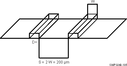
      GUID-7DAA6C9F-CE6E-4143-B006-7A9CF3DE4F14-low.gifFigure 9-1 Ground Guard Illustration
  • Length matching (unless otherwise specified):
    • For bus or traces at frequencies less than 10 MHz, the trace length matching (maximum length difference between the longest and the shortest lines) must be less than 25 mm.
    • For bus or traces at frequencies greater than 10 MHz, the trace length matching (maximum length difference between the longest and the shortest lines) must be less than 2.5 mm.
  • Characteristic impedance
    • Unless otherwise specified, the characteristic impedance for single-ended interfaces is recommended to be between 35-Ω and 65-Ω.
  • Multiple peripheral support
    • For interfaces where multiple peripherals have to be supported in the star topology, the length of each branch has to be balanced. Before closing the PCB design, it is highly recommended to verify signal integrity based on simulations including actual PCB extraction.