SLLS103P December 1990 – March 2024 AM26C31
PRODUCTION DATA
- 1
- 1 Features
- 2 Applications
- 3 Description
- 4 Pin Configuration and Functions
-
5 Specifications
- 5.1 Absolute Maximum Ratings
- 5.2 ESD Ratings
- 5.3 Recommended Operating Conditions
- 5.4 Thermal Information
- 5.5 Electrical Characteristics: AM26C31C and AM26C31I
- 5.6 Electrical Characteristics: AM26C31Q and AM26C31M
- 5.7 Switching Characteristics: AM26C31C and AM26C31I
- 5.8 Switching Characteristics: AM26C31Q and AM26C31M
- 5.9 Typical Characteristics
- 6 Parameter Measurement Information
- 7 Detailed Description
- 8 Application Information Disclaimer
- 9 Device and Documentation Support
- 10Revision History
- 11Mechanical, Packaging, and Orderable Information
Package Options
Mechanical Data (Package|Pins)
Thermal pad, mechanical data (Package|Pins)
Orderable Information
3 Description
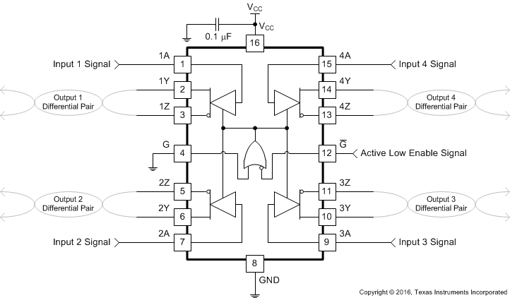
The AM26C31 device is a differential line driver with complementary outputs, designed to meet the requirements of TIA/EIA-422-B and ITU (formerly CCITT). The 3-state outputs have high-current capability for driving balanced lines, such as twisted-pair or parallel-wire transmission lines, and they provide the high-impedance state in the power-off condition. The enable functions are common to all four drivers and offer the choice of an active-high (G) or active-low ( G) enable input. BiCMOS circuitry reduces power consumption without sacrificing speed.
The AM26C31C device is characterized for operation from 0°C to 70°C, the AM26C31I device is characterized for operation from –40°C to +85°C, the AM26C31Q device is characterized for operation over the automotive temperature range of –40°C to +125°C, and the AM26C31M device is characterized for operation over the full military temperature range of –55°C to +125°C.
| PART NUMBER | PACKAGE(1) | PACKAGE SIZE(2) |
|---|---|---|
| AM26C31 | CDIP (J, 16) | 19.56mm × 6.92mm |
| PDIP (N, 16) | 19.3mm × 6.35mm | |
| SO (NS, 16) | 10.3mm × 5.3mm | |
| CFP (W, 16) | 10.3mm × 6.73mm | |
| SOIC (D, 16) | 9.9mm × 3.91mm | |
| SSOP (DB, 16) | 6.2mm × 5.3mm | |
| TSSOP (PW, 16) | 5.mm × 4.4mm | |
| LCCC (FK, 20) | 8.89mm × 8.89mm |
 Common Application Diagram