SLLS201I May 1995 – April 2024 AM26LV31
PRODUCTION DATA
- 1
- 1 Features
- 2 Applications
- 3 Description
- 4 Pin Configuration and Functions
- 5 Specifications
- 6 Parameter Measurement Information
- 7 Detailed Description
- 8 Application and Implementation
- 9 Device and Documentation Support
- 10Revision History
- 11Mechanical, Packaging, and Orderable Information
Package Options
Refer to the PDF data sheet for device specific package drawings
Mechanical Data (Package|Pins)
- NS|16
- D|16
Thermal pad, mechanical data (Package|Pins)
- D|16
Orderable Information
3 Description
The AM26LV31C and AM26LV31I are BiCMOS quadruple differential line drivers with 3-state outputs. They are designed to be similar to TIA/EIA-422-B and ITU Recommendation V.11 drivers with reduced supply-voltage range.
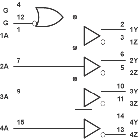
The devices are optimized for balanced-bus transmission at switching rates up to 32MHz. The outputs have very high current capability for driving balanced lines such as twisted-pair transmission lines and provide a high impedance in the power-off condition. The enable function is common to all four drivers and offers the choice of active-high or active-low enable inputs. The AM26LV31C and AM26LV31I are designed using Texas Instruments proprietary LinIMPACT-C60™ technology, facilitating ultra-low power consumption without sacrificing speed. These devices offer optimum performance when used with the AM26LV32 quadruple line receivers.
The AM26LV31C is characterized for operation from 0°C to 70°C. The AM26LV31I is characterized for operation from –45°C to 85°.C
| PART NUMBER | PACKAGE(1) | PACKAGE SIZE(2) |
|---|---|---|
| AM26LV31C | SOIC (D) 16 | 9.9mm x 6mm |
| AM26LV31I | SOIC (D) 16 | 9.9mm x 6mm |
| SO (NS) 16 | 10.2mm x 7.8mm |
 Logic Diagram (Positive Logic)