SLLS849E april 2008 – august 2023 AM26LV32E
PRODUCTION DATA
- 1
- 1 Features
- 2 Applications
- 3 Description
- 4 Revision History
- 5 Pin Configuration and Functions
- 6 Specifications
- 7 Parameter Measurement Information
- 8 Detailed Description
- 9 Application Information Disclaimer
- 10Power Supply Recommendations
- 11Layout
- 12Device and Documentation Support
- 13Mechanical, Packaging, and Orderable Information
Package Options
Mechanical Data (Package|Pins)
Thermal pad, mechanical data (Package|Pins)
Orderable Information
3 Description
The AM26LV32E device consists of quadruple differential line receivers with 3-state outputs. This device is designed to meet TIA/EIA-422-B and ITU recommendation V.11 drivers with reduced supply voltage. The device is optimized for balanced bus transmission at switching rates up to 32 MHz. The 3-state outputs permit connection directly to a bus-organized system. The AM26LV32E has an internal fail-safe circuitry that prevents the device from putting an unknown voltage signal at the receiver outputs. In the open fail-safe, a high state is produced at the respective output. This device is supported for partial-power-down applications using Ioff. Ioff circuitry disables the outputs, preventing damaging current back-flow through the device when it is powered down.
| PART NUMBER | PACKAGE(1) | PACKAGE SIZE(2) |
|---|---|---|
| AM26LV32E | SO (16) | 10.2 mm × 7.8 mm |
| SOIC (16) | 9.9 mm x 6 mm | |
| VQFN (16) | 4 mm x 3.5 mm | |
| TSSOP (16) | 5 mm x 6.4 mm |
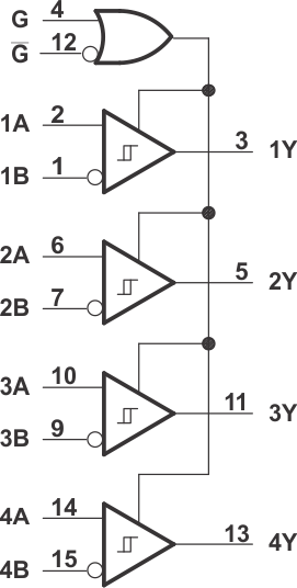
 Logic Diagram (Positive Logic)