SBAS562B April 2012 – December 2019 AMC1100
PRODUCTION DATA.
- 1 Features
- 2 Applications
- 3 Description
- 4 Revision History
- 5 Pin Configuration and Functions
-
6 Specifications
- 6.1 Absolute Maximum Ratings
- 6.2 ESD Ratings
- 6.3 Recommended Operating Conditions
- 6.4 Thermal Information
- 6.5 Power Ratings
- 6.6 Insulation Specifications
- 6.7 Safety-Related Certifications
- 6.8 Safety Limiting Values
- 6.9 Electrical Characteristics
- 6.10 Insulation Characteristics Curves
- 6.11 Typical Characteristics
- 7 Detailed Description
- 8 Application and Implementation
- 9 Power Supply Recommendations
- 10Layout
- 11Device and Documentation Support
- 12Mechanical, Packaging, and Orderable Information
Package Options
Mechanical Data (Package|Pins)
Thermal pad, mechanical data (Package|Pins)
- DUB|8
Orderable Information
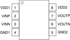
5 Pin Configuration and Functions
DUB and DWV Packages
SOP-8 and SOIC-8
(Top View)

Pin Descriptions
| PIN | FUNCTION | DESCRIPTION | |
|---|---|---|---|
| NAME | NO. | ||
| GND1 | 4 | Power | High-side analog ground |
| GND2 | 5 | Power | Low-side analog ground |
| VDD1 | 1 | Power | High-side power supply |
| VDD2 | 8 | Power | Low-side power supply |
| VINN | 3 | Analog input | Inverting analog input |
| VINP | 2 | Analog input | Noninverting analog input |
| VOUTN | 6 | Analog output | Inverting analog output |
| VOUTP | 7 | Analog output | Noninverting analog output |