SBAS789B October 2017 – April 2020 AMC1106E05 , AMC1106M05
PRODUCTION DATA.
- 1 Features
- 2 Applications
- 3 Description
- 4 Revision History
- 5 Device Comparison Table
- 6 Pin Configuration and Functions
-
7 Specifications
- 7.1 Absolute Maximum Ratings
- 7.2 ESD Ratings
- 7.3 Recommended Operating Conditions
- 7.4 Thermal Information
- 7.5 Power Ratings
- 7.6 Insulation Specifications
- 7.7 Safety-Related Certifications
- 7.8 Safety Limiting Values
- 7.9 Electrical Characteristics: AMC1106x
- 7.10 Timing Requirements
- 7.11 Switching Characteristics
- 7.12 Insulation Characteristics Curves
- 7.13 Typical Characteristics
- 8 Detailed Description
- 9 Application and Implementation
- 10Power Supply Recommendations
- 11Layout
- 12Device and Documentation Support
- 13Mechanical, Packaging, and Orderable Information
Package Options
Mechanical Data (Package|Pins)
- DWV|8
Thermal pad, mechanical data (Package|Pins)
Orderable Information
9.2.2 Detailed Design Procedure
The high-side power supply (AVDD) for the AMC1106 is externally derived from either a capacitive-drop or a coreless transformer power-supply circuit. Further details are provided in the Power Supply Recommendations section.
The floating ground reference (AGND) is derived from one of the ends of the shunt resistor that is connected to the analog inputs of the AMC1106. If a four-pin shunt is used, the inputs of the device are connected to the inner leads and AGND is connected to one of the outer shunt leads.
Use Ohm's Law to calculate the voltage drop across the shunt resistor (VSHUNT) for the desired measured current: VSHUNT = I × RSHUNT.
Consider the following two restrictions to choose the proper value of the shunt resistor RSHUNT:
- The voltage drop caused by the nominal current range must not exceed the recommended differential input voltage range: VSHUNT ≤ ±50 mV
- The voltage drop caused by the maximum allowed overcurrent must not exceed the input voltage that causes a clipping output: |VSHUNT| ≤ |VClipping|
Use an RC filter in front of the AMC1106 to improve the overall signal-to-noise performance of the system and improve the immunity of the circuit to high-frequency electromagnetic fields.
For the AMC1106 output bitstream averaging, a poly-phase device version from TI's MSP430F67x family of low-power microcontrollers (MCUs) is recommended. This family offers the sigma-delta module (SD24_B) that allows for bypassing the internal modulator and directly accessing the digital filter. The integrated trigger and clock generator support synchronization of all three AMC1106 devices and the internal 10-bit SAR ADC that is used to deliver the voltage information of all phases.
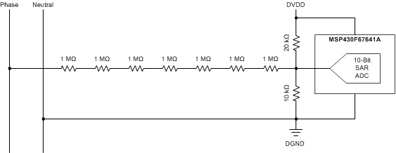
Figure 50 shows a voltage divider circuit with a common-mode set to 1/3 of the supply voltage that is used to adjust the mains voltage signal to the input voltage range of the SAR ADC used in the MSP430F67641A.
 Figure 50. Level-Shifted Voltage Divider
 For further design recommendations and system level considerations, see the Multi-Phase Power Quality Measurement With Isolated Shunt Sensors or the Magnetically Immune Transformerless Power Supply for Isolated Shunt Current Measurement reference designs offered by TI.