SBAS771C June 2017 – February 2020 AMC1303E0510 , AMC1303E0520 , AMC1303E2510 , AMC1303E2520 , AMC1303M0510 , AMC1303M0520 , AMC1303M2510 , AMC1303M2520
PRODUCTION DATA.
- 1 Features
- 2 Applications
- 3 Description
- 4 Revision History
- 5 Device Comparison Table
- 6 Pin Configuration and Functions
-
7 Specifications
- 7.1 Absolute Maximum Ratings
- 7.2 ESD Ratings
- 7.3 Recommended Operating Conditions
- 7.4 Thermal Information
- 7.5 Power Ratings
- 7.6 Insulation Specifications
- 7.7 Safety-Related Certifications
- 7.8 Safety Limiting Values
- 7.9 Electrical Characteristics: AMC1303x05x
- 7.10 Electrical Characteristics: AMC1303x25x
- 7.11 Switching Characteristics
- 7.12 Insulation Characteristics Curves
- 7.13 Typical Characteristics
- 8 Detailed Description
- 9 Application and Implementation
- 10Power Supply Recommendations
- 11Layout
- 12Device and Documentation Support
- 13Mechanical, Packaging, and Orderable Information
Package Options
Mechanical Data (Package|Pins)
- DWV|8
Thermal pad, mechanical data (Package|Pins)
Orderable Information
7.11 Switching Characteristics
over operating ambient temperature range (unless otherwise noted)| PARAMETER | TEST CONDITIONS | MIN | TYP | MAX | UNIT | |
|---|---|---|---|---|---|---|
| fCLK | Internal clock frequency,
on the CLKOUT pin of the AMC1303Mx only |
AMC1303Mxx10 | 9.6 | 10 | 10.4 | MHz |
| AMC1303Mxx20 | 19.2 | 20 | 20.8 | |||
| Duty Cycle | Internal clock duty cycle(1),
on the CLKOUT pin of the AMC1303Mx only |
45% | 50% | 55% | ||
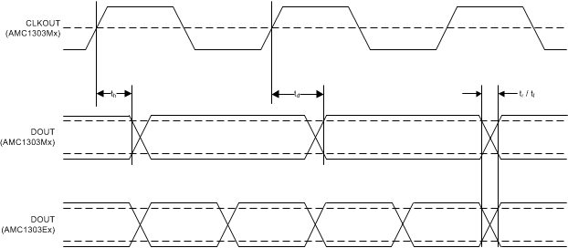
| th | DOUT hold time after rising edge of CLKOUT | AMC1303Mx, CLOAD = 15 pF | 7 | ns | ||
| td | DOUT delay time after rising edge of CLKOUT | AMC1303Mx, CLOAD = 15 pF | 15 | ns | ||
| tr | DOUT, CLKOUT rise time | 10% to 90%, 2.7 V ≤ DVDD ≤ 3.6 V, CLOAD = 15 pF | 0.8 | 3.5 | ns | |
| 10% to 90%, 4.5 V ≤ DVDD ≤ 5.5 V, CLOAD = 15 pF | 1.8 | 3.9 | ||||
| tf | DOUT, CLKOUT fall time | 90% to 10%, 2.7 V ≤ DVDD ≤ 3.6 V, CLOAD = 15 pF | 0.8 | 3.5 | ns | |
| 90% to 10%, 4.5 V ≤ DVDD ≤ 5.5 V, CLOAD = 15 pF | 1.8 | 3.9 | ||||
| tASTART | Analog startup time | AVDD step to 3.0 V with DVDD ≥ 2.7 V | 0.5 | ms | ||
(1) Duty cycle values are specified by design.
 Figure 1. AMC1303Mx Digital Interface Timing
  Figure 2. Digital Interface Startup Timing