SBAS771C June 2017 – February 2020 AMC1303E0510 , AMC1303E0520 , AMC1303E2510 , AMC1303E2520 , AMC1303M0510 , AMC1303M0520 , AMC1303M2510 , AMC1303M2520
PRODUCTION DATA.
- 1 Features
- 2 Applications
- 3 Description
- 4 Revision History
- 5 Device Comparison Table
- 6 Pin Configuration and Functions
-
7 Specifications
- 7.1 Absolute Maximum Ratings
- 7.2 ESD Ratings
- 7.3 Recommended Operating Conditions
- 7.4 Thermal Information
- 7.5 Power Ratings
- 7.6 Insulation Specifications
- 7.7 Safety-Related Certifications
- 7.8 Safety Limiting Values
- 7.9 Electrical Characteristics: AMC1303x05x
- 7.10 Electrical Characteristics: AMC1303x25x
- 7.11 Switching Characteristics
- 7.12 Insulation Characteristics Curves
- 7.13 Typical Characteristics
- 8 Detailed Description
- 9 Application and Implementation
- 10Power Supply Recommendations
- 11Layout
- 12Device and Documentation Support
- 13Mechanical, Packaging, and Orderable Information
Package Options
Mechanical Data (Package|Pins)
- DWV|8
Thermal pad, mechanical data (Package|Pins)
Orderable Information
6 Pin Configuration and Functions
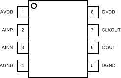
AMC1303Mx: DWV Package
8-Pin SOIC
Top View

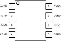
AMC1303Ex: DWV Package
8-Pin SOIC
Top View

Pin Functions
| NAME | AMC1303Mx | AMC1303Ex | I/O | DESCRIPTION |
|---|---|---|---|---|
| AGND | 4 | 4 | — | Analog (high-side) ground reference |
| AINN | 3 | 3 | I | Inverting analog input |
| AINP | 2 | 2 | I | Noninverting analog input |
| AVDD | 1 | 1 | — | Analog (high-side) power supply, 3.0 V to 5.5 V.
See the Power Supply Recommendations section for decoupling recommendations. |
| CLKOUT | 7 | — | O | Modulator clock output, 10 MHz (on AMC1303Mxx10) or 20 MHz (on AMC1303Mxx20) nominal |
| DGND | 5 | 5 | — | Digital (controller-side) ground reference |
| DGND | — | 7 | — | Connect this pin to the controller-side ground for AMC1303Ex derivates |
| DOUT | 6 | 6 | O | Modulator bitstream output. This pin is a Manchester coded output for the AMC1303Ex derivates. |
| DVDD | 8 | 8 | — | Digital (controller-side) power supply, 2.7 V to 5.5 V.
See the Power Supply Recommendations section for decoupling recommendations. |